semi合集-English.pdf - 第7714页
SEMI T10-0701 © SEMI 2001 7 7.5.3 Data Matrix Cell Height 7.5.3.1 Compute the Data Matrix Cell H ei ght (DMCH) us ing the distance betw ee n P1 and P2, dist(P1,P2), th e distance betw een P3 and P 4, dist(P3,P4) an d the…
SEMI T10-0701 © SEMI 2001 6
7.4 Mark Growth
7.4.1 Mark Growth is concerned wit h tracking the
tendency of a marking system to over or under mark the
symbol. This is a size comparison between the actual
marked cells vs. their nominal size. Changes in mark
growth can be indicative of changes in the marking
process or substrate characteristics or changes in the
reader configuration, such as illumination or optical
focus.
7.4.2
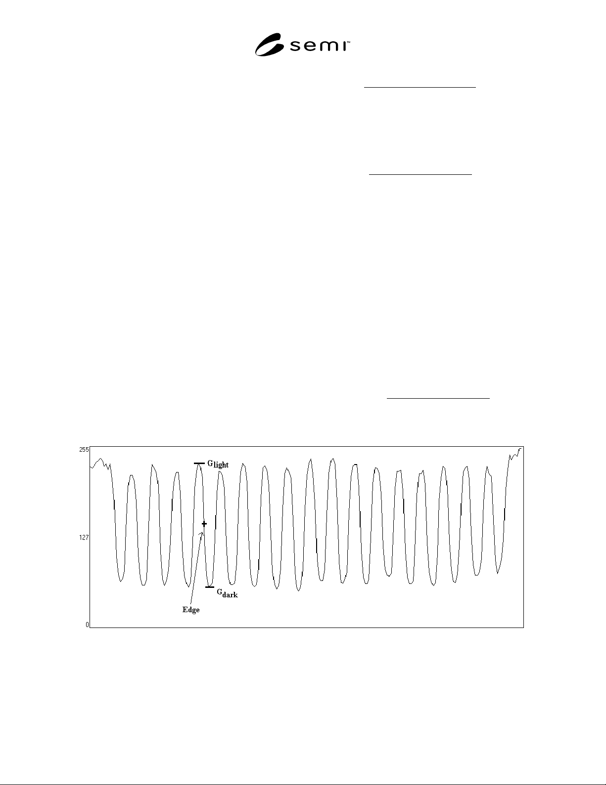
Within the grayscale image, ba sed upon the
matrix coordinates and the number of rows and
columns in the matrix, determine a scanline of pixels
which bisects the horizontal alternating pattern and
determine a scanline which bisects the vertical
alternating pattern of the matrix (Figure 3). Scan along
each alternating pattern, generating a cross-sectional
grayscale profile of each alternating pattern as shown in
Figure 5. Determine the location of each edge within
the alternating patterns locally, using an appropriate
edge detection method. Based upon the edge locations,
compute the width of each matrix cell in the horizontal
alternating pattern in the direction of the horizontal
scanline. Also, compute the height of each matrix cell
in the vertical alternating pattern in the direction of the
vertical scanline. Separate the mark and space cell
widths and compute the median space cell width (SCW)
and the median mark cell width (MCW). Horizontal
Mark Growth (HMG) is computed as:
100%
(SCW) Med(MCW) Med
MCW) ( Med
HMG ×
+
= (3)
Separate the mark and space cell heights and compute
the median space cell height (SCH) and the median
mark cell height (MCH). Vertical Mark Growth
(VMG) is computed as:
100%
Med(SCH)Med(MCH)
Med(MCH)
VMG ×
+
= (4)
Report the Horizontal Mark Growth and Vertical Mark
Growth values.
7.5 Data Matrix Cell Size
7.5.1 The Data Matrix Cell Size expresses the average
size of each cell in the matrix in pixels and is composed
of a width and height component. Compute the Cell
Size using the distances between corner points and the
known number of rows M and the known number of
columns N in the matrix (referring to Figure 3).
7.5.2
Data Matrix Cell Width
7.5.2.1 Compute the Data Matrix Cell Width
(DMCW) using the distance between P1 and P4,
dist(P1, P4), the distance between P2 and P3, dist(P2,
P3) and the number of columns N as follows:
N2
P3)(P2,dist P4)(P1,dist
DMCW
×
+
=
(5)
Report the Data Matrix Cell Width.
Figure 5
Mark Growth Cross-Sectional Grayscale Profile

SEMI T10-0701 © SEMI 20017
7.5.3 Data Matrix Cell Height
7.5.3.1 Compute the Data Matrix Cell Height
(DMCH) using the distance between P1 and P2,
dist(P1,P2), the distance between P3 and P4,
dist(P3,P4) and the number of rows M as follows:
M2
P4)dist(P3,P2)dist(P1,
DMCH
×
+
=
(6)
Report the Data Matrix Cell Height.
7.6 Data Matrix Mark Misplaceme nt
7.6.1 Data Matrix Mark Misplacement measures the
average misplacement of Data Matrix marks from their
respective ideal Data Matrix Cell Center Points as
defined in Section 7.1.3. The Mark Misplacement is
measured separately in horizontal and vertical
directions relative to the average width of the marks in
the respective direction.
7.6.2
Using the mark cell horizontal and vertical edge
locations, as determined in Section 7.4.2, compute the
image coordinate of the midpoint between the edges of
each mark in the corresponding horizontal and vertical
directions. In the horizontal direction, for each mark
calculate its misplacement MH
i
as the distance between
the detected midpoint and its ideal cell center point. In
the vertical direction, for each mark calculate its
misplacement MV
i
as the distance between the detected
midpoint and its ideal cell center point.
7.6.3
Horizontal Mark Misplacemen t
7.6.3.1 In the horizontal direction, for a given number
of columns N, and the Data Matrix Cell Width
(DMCW) as computed in Section 7.5.2, compute the
Horizontal Mark Misplacement (HMM)as follows:
100%
DMCWn
n
1i
i
MH
HMM ×
×
=
= (7)
where n = N/2 if N is even or n = N/2+1 if N is odd.
Report the Horizontal Mark Misplacement.
7.6.4
Vertical Mark Misplacement
7.6.4.1 In the vertical direction, for a g iven number of
rows M, and the Data Matrix Cell Height (DMCH) as
computed in Section 7.5.3, compute the Vertical Mark
Misplacement (VMM) as follows:
100%
DMCHm
m
1i
i
MV
VMM ×
×
=
= (8)
where m = M/2 if M is even and m = M/2+1 if M is
odd. Report the Vertical Mark Misplacement.
7.7 Unused Error Correction
7.7.1 The error correction capacity of Reed-Solomon
decoding is expressed in the equation:
pdte −≤+ 2
where: (9)
e is the number of erasures,
t is the number of errors,
d is the number of error correction codewords,
p is the number of codewords reserved for
error detection.
7.7.2 Values for d and p are defined by the AIMI
Symbology Specification (often depending on symbol
size), while e and t are determined during a successful
decode. Compute the Unused Error Correction as
follows:
()
()
100%
pd
2te
1.0UEC ×
−
+
−=
ö
ç
ç
è
æ
(10)
Report the Unused Error Correction value.
7.7.3
In symbols with more than one (e.g. interleaved)
Reed-Solomon block, calculate the Unused Error
Correction for each block independently and report the
value for each block.
7.8
Cell Defects and Finder Patter n Defects
7.8.1 If the error correction capacity of the Data
Matrix symbol is not exceeded then the Cell Defect
measurement can be made. Because the Data Matrix
symbol has been decoded, the correct binary value of
each cell is known.
7.8.2
Based upon the Data Matrix Grid as defined in
Section 7.1.2 (Figure 4), and the total matrix size,
identify the number and location of all pixels which fall
within the bounds of the Data Matrix Grid. Based upon
the reflectance threshold determined by the Symbol
Contrast measurement, assign a binary value to each
pixel within the Data Matrix Grid. Accumulate the
total number of identified image pixels, which are the
incorrect binary value. Divide this number by the total
number of pixels within the Data Matrix Grid.
100%
pixelsof#total
pixelsincorrectof#
DefectsCell ×= (11)
7.8.3 Finder pattern quality can be c alculated in a
similar manner. Based on the Data Matrix Grid as
defined in Section 7.1.2 (Figure 4), determine the
number and location of image pixels which fall within
the bounds of the L finder pattern of the Data Matrix
Grid. Using the reflectance threshold determined by
the Symbol Contrast measurement, assign a binary
value to each pixel within the L finder pattern.
Accumulate the total number of identified image pixels,

SEMI T10-0701 © SEMI 2001 8
which are the incorrect binary value. Divide this
number by the total number of pixels within the L
finder pattern.
100%
pixelsof#total
pixelsincorrectof#
DefectsF.P. ×= (12)
8 Interpretation of Results
8.1 Result Significance
8.1.1 The significance of the assessment results will
depend on the mark/reader application. Open system
applications in which multiple marker and reader
systems of various types at multiple sites are used will
require stricter adherence to desired mark assessment
results. If the mark is intended to survive subsequent
processing steps after marking which will affect mark
characteristics, then reassessment may be necessary to
ensure continued readability.
9 Reporting Results
9.1 Assessment Results
9.1.1 The results of each assessment shall be reported
and listed individually.
9.2 Additional Information
9.2.1 The following items should als o appear in the
report:
• identification of the mark under assessment;
• operator identification;
•
location of where the assessment was done;
• description of specific marking and reading
equipment used.
9.3 Supplemental Information
9.3.1 Supplemental information can be reported
optionally. This information provides further details
about the size, content and color polarity of the Data
Matrix symbol.
9.3.2
Symbol Type indicates the ECC (error
correction) level of the analyzed symbol. See the AIMI
Specification for details on ECC levels other than ECC
200.
9.3.3
Symbol Size indicates the tota l size of the
matrix, including the L and alternating patterns per the
AIMI specification.
9.3.4 Image Polarity can be Dark on Light or Light on
Dark. The first term refers to the polarity of the L, the
second the polarity of the quiet zone.
9.3.5 Encoded Data shows the printa ble encoded
characters only. As many lines as needed will be
included for larger symbols.
9.3.6
Data Codewords and Error Co dewords (ECC
200 only) shows the actual encoding codewords that are
contained in the symbol. Codewords, which contain
errors, may be indicated or highlighted. By referring to
Annex M of the AIMI Specification the exact physical
location of codewords can be determined.
9.3.7
Encodation Scheme (ECC 0 through 140 only)
reports the “Base” number, which relates to the density
or efficiency with which the data has been encoded in
the symbol. For more detailed information refer to
Section 5 of the AIMI Specification.
10 Precision and Accuracy
10.1 Pixel Resolution
10.1.1 The pixel resolution shall be sp ecified for all
assessments. This value determines the precision,
accuracy and repeatability of each resulting
measurement.
NOTICE: SEMI makes no warranties or
representations as to the suitability of the standard set
forth herein for any particular application. The
determination of the suitability of the standard is solely
the responsibility of the user. Users are cautioned to
refer to manufacturer’s instructions, product labels,
product data sheets, and other relevant literature
respecting any materials mentioned herein. These
standards are subject to change without notice.
The user's attention is called to the possibility that
compliance with this standard may require the use of
copyrighted material or of an invention covered by
patent rights. RVSI Acuity CiMatrix has filed a
statement with SEMI asserting that the patented or
copyrighted item can be used by the public for the
purpose of implementing this standard without specific
license and without payment of royalty or other charge.
Attention is also drawn to the possibility that some
elements of this standard may be subject to patented
technology or copyrighted items other than those
identified above. Semiconductor Equipment and
Materials International (SEMI) shall not be held
responsible for identifying any or all such patented
technology or copyrighted items. By publication of this
standard, SEMI takes no position respecting the validity
of any patent rights or copyrights asserted in connection
with any item mentioned in this standard. Users of this
standard are expressly advised that determination of
any such patent rights or copyrights and the risk of
infringement of such rights are entirely their own
responsibility.
Copyright by SEMI® (Semiconductor Equipment and Materials
International), 3081 Zanker Road, San Jose, CA 95134. Reproduction o
f
the contents in whole or in part is forbidden without express written
consent of SEMI.