semi合集-English.pdf - 第6271页
SEMI G53-92 © SEMI 1992 3 Lid Size Lid T hickness* Preform Thickness Preform Wi dth Pkg.S/r Wi dth Corner Radii <0.251" 0.010" 0.0015– 0.0021" 0.025" m in. 0.0425" m in. 0.020–m in. 0.251–0. 5…
SEMI G53-92 © SEMI 1992 2
protrusion — an adherent fragment of excess material
on the surface of lid or preform.
scratch — surface mark which exposes underlying
metal.
seal ring — area designated for attaching the lid to the
package by welding or soldering techniques.
stain — a two-dimensional substance on a surface of
the lid or preform.
tack weld — small spot welds, generally located in the
corners which are used to attach the preform to the lid.
void — absence of plating from designated area.
weld splatter — melted preform material which extends
from the weld.
4 Ordering Information
Purchase orders for metal lid/preform assemblies
furnished to this specification shall include the
following information.
4.1 Current customer drawing revision detailing:
All dimensions and tolerances per ANSI Y14.5M
Base material and hardness
Type, and thickness of the plating(s)
Preform type and composition
4.2 Reference to this specification.
4.3 Supplier certification requirements
4.4 Any additions to, or variations from, this
specification.
5 Materials
The definitions, design guidelines, defect criteria, and
functional tests described in this specification relate to
lid/preform assemblies made with the following
materials.
5.1 Lid
5.1.1 Base material to be Iron Nickel Cobalt alloy per
MIL-M-38510, Type A; OR Iron Nickel alloy per MIL-
M-38510, Type B unless otherwise stated on the
purchase order.
5.1.2 Plating shall meet the requirements of MIL-M-
38510 unless otherwise stated in the purchasing
document.
5.2 Preform
5.2.1 Preform to be 80% (+0/-1% tolerance) gold,
balance to be tin unless otherwise stated on the
purchase order. Gold and tin to be 99.99% pure per
ASTM E 29.
Maximum Trace Elements
Silver (Ag) 100 ppm
Copper (Cu) 50 ppm
Lead (Pb) 50 ppm
Palladium (Pd) 20 ppm
Iron (Fe) 10 ppm
Others 10 ppm each
Total all impurities: 149 ppm
6 Design Guidelines
These guidelines are based on the use of a furnace
sealing process, not seam sealing.
6.1 General Guidelines
6.1.1 The I.D. of the lid preform should be 0.010
larger than the package seal ring I.D. as long as preform
width specifications are not violated.
6.1.2 The O.D. of the lid should be 0.025" to 0.035"
smaller than the package seal ring O.D. as long as
preform width specifications are not violated.
NOTE: The dimensions listed are based on nominal
tolerances only. The worst case package and lid conditions
must be considered.
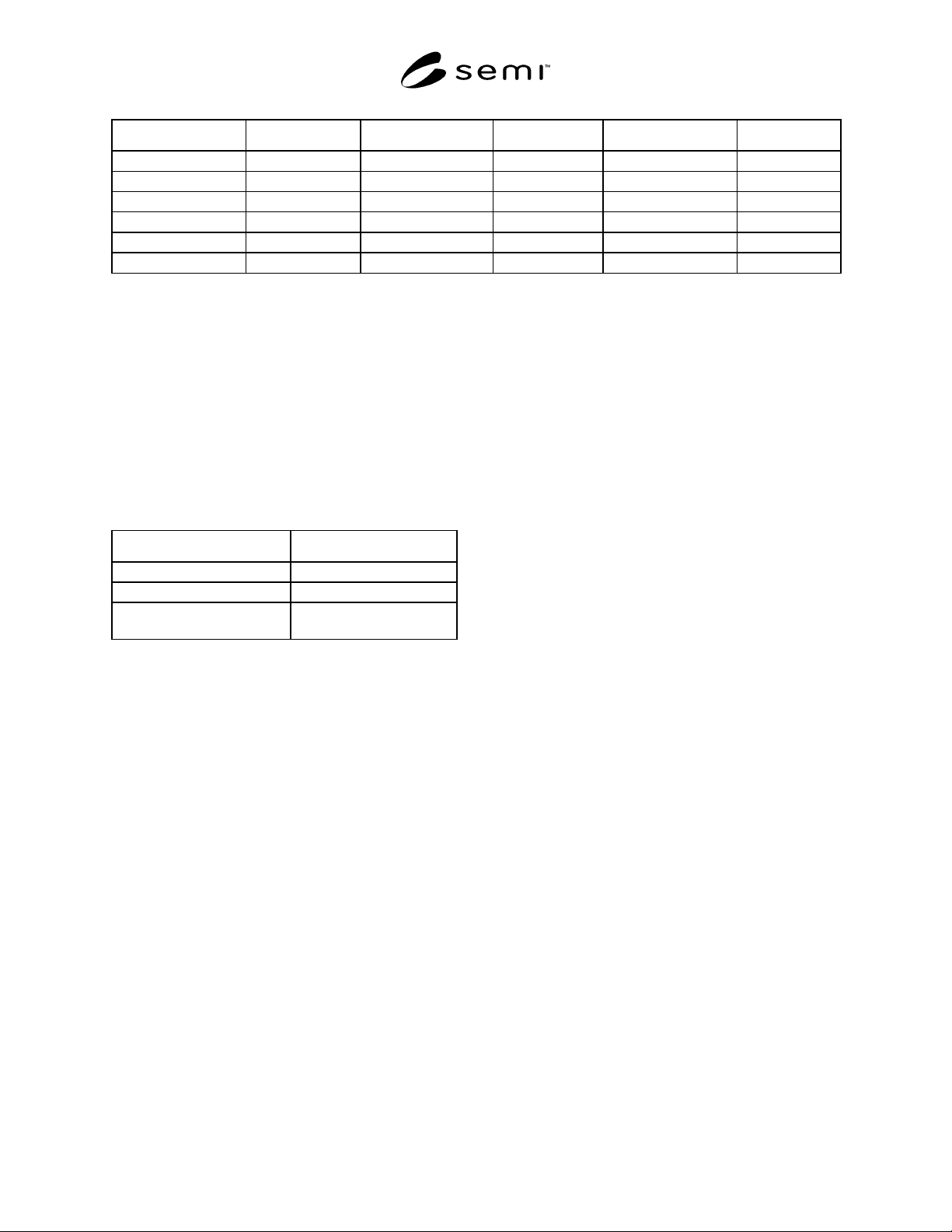
6.1.3 Recommendations — The following table is a
guideline only. Specific requirements may differ
depending on the package type or style.
SEMI G53-92 © SEMI 19923
Lid Size Lid Thickness* Preform Thickness Preform Width Pkg.S/r Width Corner Radii
<0.251" 0.010" 0.0015–0.0021" 0.025" min. 0.0425" min. 0.020–min.
0.251–0.500" 0.010" 0.0021" 0.035" min. 0.0525" min. "
0.501–0.650" 0.010–0.015" 0.0021–0.0024" 0.035" min. 0.0525" min. "
0.651–1.000" 0.015" 0.0021–0.0030" 0.040–0.060" 0.0625–0.0675" "
1.001–1.250" 0.015" 0.0021–0.0030" 0.045–0.065" 0.0675–0.0725 "
>1.250" 0.015" 0.0021–0.0030" 0.050" min. 0.0725" min. "
* Tolerance for Lid Thickness is ± 10 %.
** Tolerance for Preform Thickness is ± 0.0003".
7 Defect Limits
Visual inspection shall be carried out at 3×
magnification with verifiaction at 10×.
alpha emission — Alpha Emission Level Max: 0.05
counts/cm
2
/hour +30/-0 seconds. Test method to be
agreed upon between user and supplier.
blisters/peeling — None allowed after 3 minutes dwell
time at 400 ± 10°C in air.
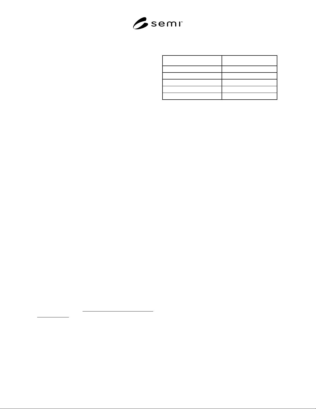
bow — Preform bow not to exceed:
Lid Size Maximum Allowable Bow
< 0.500" 0.003"
0.501 – 1.500" 0.005"
1.500" and above To be determined between
supplier and user.
burrs (stamping) — None allowed greater than 0.001"
in height.
chipouts — Chipouts exceeding 10% of the width of
the preform (may be up to 20% in the corner) are not
allowed. No chipouts allowed in lid.
cracks — Cracks in the lid not allowed. The preform
shall not be broken, except in such cases where both
sides of the break are in contact, and the preform is flat
and firmly attached to the lid. Maximum of one
(allowable) crack per preform allowed.
discoloration/stains — Discoloration of the finish shall
not be cause for rejection unless there is evidence of
corrosion or other contamination.
flatness — Lid must be flat within 0.001" per 0.500"
T.I.R.
foreign material/contamination — Adherent material
which cannot be removed by blowing with 20 psi air or
nitrogen is not allowed.
pits — Pits larger than 0.005" are not allowed. No more
than three acceptable pits are allowed on either surface
of the lid and there must be a minimum of 0.030"
between sites. Pits must not have exposed base metal.
NOTE: A sample of lids with pits may be subjected to Salt
Atmosphere test per MIL-STD 883, Method 1009, Condition
A as a condition of lot acceptance.
plating voids — No plating voids greater than .005" in
any dimension. Lids with smaller plating voids may be
subjected to Salt Atmosphere Test as described above
as a condition of lot acceptance.
preform alignment — Misalignment shall not exceed
0.005" from any one edge of the lid.
preform attachment — Preform to be firmly attached to
the lid in at least 3 corner locations.
protrusions — Protrusions larger than 0.005" in any
horizontal dimension or 0.001" in height are not
allowed.
scratches — Scratches which expose base metal not
allowed.
tack weld height — Must be firmly adherent and max
0.003".
7.1 All lids must meet the following criteria:
Salt atmosphere per MIL-STD 883, Method 1009,
Condition A
Resistance to Solvents per MIL-STD 883, Method 2015
Gold plating per MIL-M-38510
8 Sampling
The sampling plan shall be agreed upon between user
and supplier.
9 Incoming Inspection
9.1 Incoming inspection to be performed per user
drawing with reference to this specification.
9.1.1 Plating Thickness — Plating thickness shall be
measured by X-Ray Fluorescence per ASTM B568.
The tolerance on the thickness shall be agreed upon
between user and supplier. For multilayer plated lids,
additional layers should be measured by cross section.
SEMI G53-92 © SEMI 1992 4
9.1.2 Material Hardness — Hardness shall be
evaluated per ASTM E 384 or E 10 to limits agreed
upon between user and supplier.
9.1.3 Functional Testing
9.1.3.1 Functional testing may be performed at the
option of the user or supplier. Test to be agreed upon
between user and supplier.
9.1.3.2 Hermeticity parts should be evaluated per
MIL-STD 883, Method 1014.
9.1.4 Marking — Marking permanency shall be
evaluated per MIL-STD 883, Method 2015.
9.1.5 Corrosion Resistance — Corrosion resistance
shall be evaluated per MIL-STD 883, Method 1009
(Salt Atmosphere).
10 Certification
Upon request of the user in the purchase order, a
supplier’s certification that the product was
manufactured and tested in accordance with this
specification, together with a report of the test results,
shall be furnished at the time of shipment. Certification
to user specification may also be required. This
certification does not remove the supplier’s
responsibility for discrepant product subsequently
found by the user.
11 Packaging and Package M arking
11.1 Packaging — The shipping containers and
materials shall be suitably selected to provide the
components with protection from normal transportation
damage risks which include crushing, abrasion,
spillage, and exposure to moisture and other corrosive
gasses. The inner packing materials must be clean room
compatible as defined by user.
11.2 Package Marking
11.2.1 Internal Packages — Each internal package
shall be marked as follows:
User’s Part Number
User’s Order Number
Drawing Number (user’s and supplier’s, if appropriate)
Plating Lot Number
Manufacturing Lot Number
Quantity Date of Manufacture
External Marking — The external packing list shall
include the following details:
User’s Part Number
User’s Order Number
Quantity Shipping Date
Any specific instructions for receiving personnel
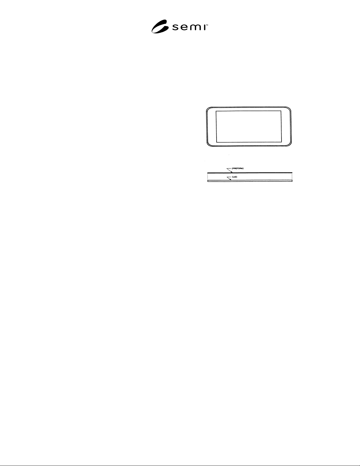
Figure 1
NOTICE: These standards do not purport to address
safety issues, if any, associated with their use. It is the
responsibility of the user of these standards to establish
appropriate safety and health practices and determine
the applicability of regulatory limitations prior to use.
SEMI makes no warranties or representations as to the
suitability of the standards set forth herein for any
particular application. The determination of the
suitability of the standard is solely the responsibility of
the user. Users are cautioned to refer to manufacturer’s
instructions, product labels, product data sheets, and
other relevant literature respecting any materials
mentioned herein. These standards are subject to
change without notice.
The user’s attention is called to the possibility that
compliance with this standard may require use of
copyrighted material or of an invention covered by
patent rights. By publication of this standard, SEMI
takes no position respecting the validity of any patent
rights or copyrights asserted in connection with any
item mentioned in this standard. Users of this standard
are expressly advised that determination of any such
patent rights or copyrights, and the risk of infringement
of such rights, are entirely their own responsibility.
Copyright by SEMI® (Semiconductor Equipment and Materials
International), 3081 Zanker Road, San Jose, CA 95134. Reproduction o
f
the contents in whole or in part is forbidden without express written
consent of SEMI.