semi合集-English.pdf - 第4947页
SEMI M11-0704 © SEMI 1988, 2004 4 Figure 2 This is a m ound that does not h ave the sharp edges of an Epitaxial St acking Fault , but is n ot as high as a Bump. They are typically s ized much smaller in a SSIS th an thei…
SEMI M11-0704 © SEMI 1988, 2004 3
• Device characteristics that may be affected —
leakage and gate oxide integrity, from
crystallographic changes.
• Detection characteristics used for characterization
— side length and depth, orientation parallel to a
<110> direction.
• Discrimination characteristics used for
characterization — shape, length ~ epi layer
thickness: 1–10 µm. Stacking faults may cluster
(see Figure 7) and scatter more than a single
stacking fault.
• Specification characteristics used for wafer
qualification — Number per wafer. Since certain
types of epi stacking faults have no observed
impact on device performance while others are
killer defects no number can be assigned without a
clear identification of the type of epi stacking fault
that is involved.
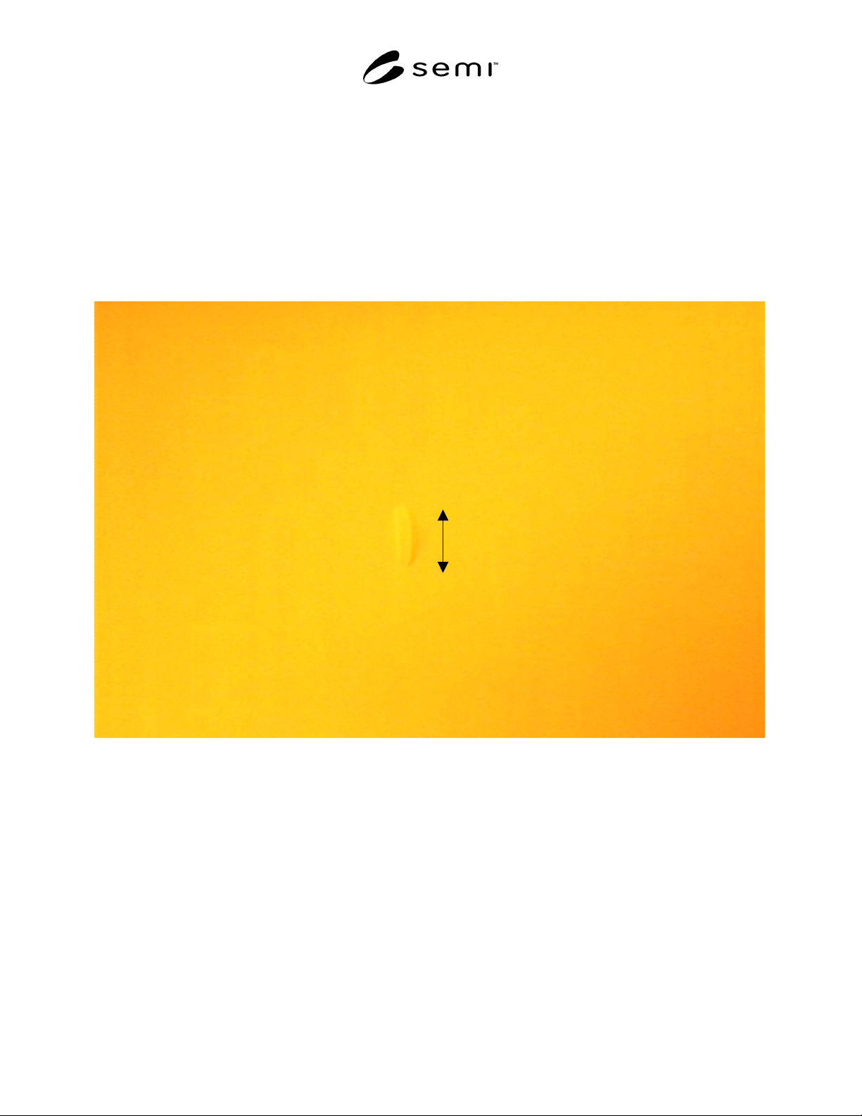
Figure 1
A Mound. Magnification 1000 times using Nomarksi Interference Microscopy. Approximate SSIS scattering
event size 0.22 µm.
23 µm
SEMI M11-0704 © SEMI 1988, 2004 4
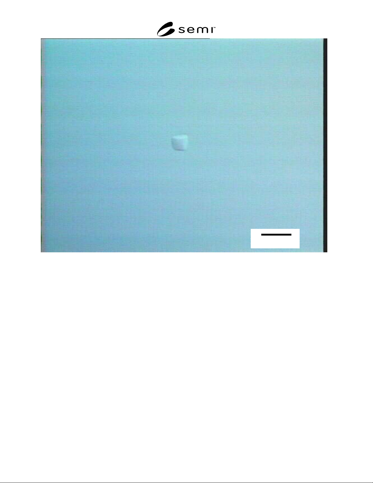
Figure 2
This is a mound that does not have the sharp edges of an Epitaxial Stacking Fault, but is not as high as a
Bump. They are typically sized much smaller in a SSIS than their actual size, but some have facets that
scatter enough light to be more easily detected. Some people refer to this feature as a hillock which is a type
of mound. The shape can be either circular or square. Magnification 500 times using Nomarski Interference
Microscopy. Approximate SSIS event size: 0.15 µm
20
µ
m
SEMI M11-0704 © SEMI 1988, 2004 5
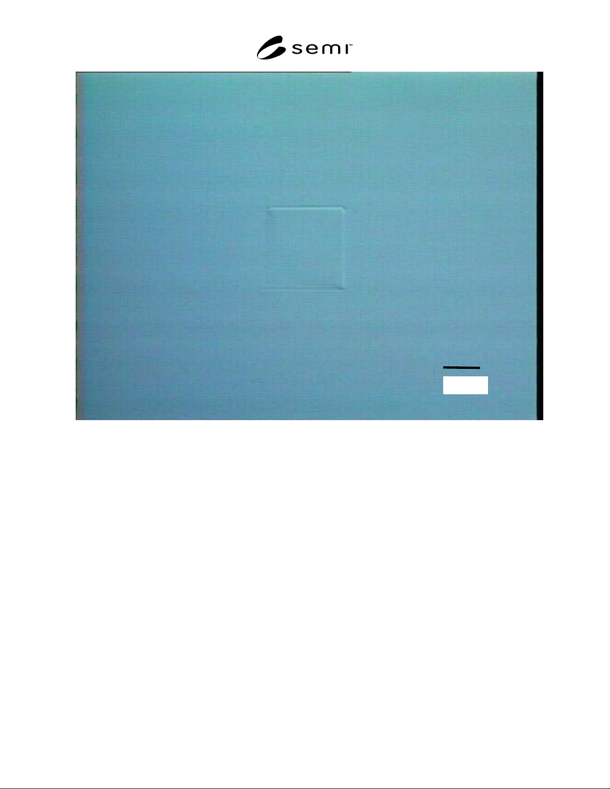
Figure 3
The Epi Stacking Fault (ESF) defect is a grown-in defect with 1 to 4 sides of a square visible. Magnification
1500 times using Nomarski Interference Microscopy. Approximate SSIS event size: 0.165 µm
5
µ
m