semi合集-English.pdf - 第5488页
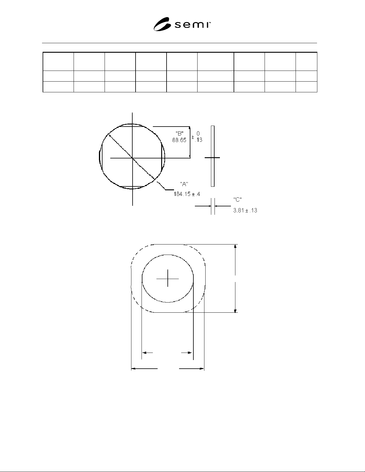
SEMI P4-92 © SEMI 1983, 1999 5 Table 5. Specification for Diameter, Flat De pth, and Thickness for R ound Substrates (proposed) Nominal Diameter Diameter (A) Mi n. Diameter (A) Ma x. Flat Depth (B) Mi n. Flat Depth (B) M…
SEMI P4-92 © SEMI 1983, 1999 4
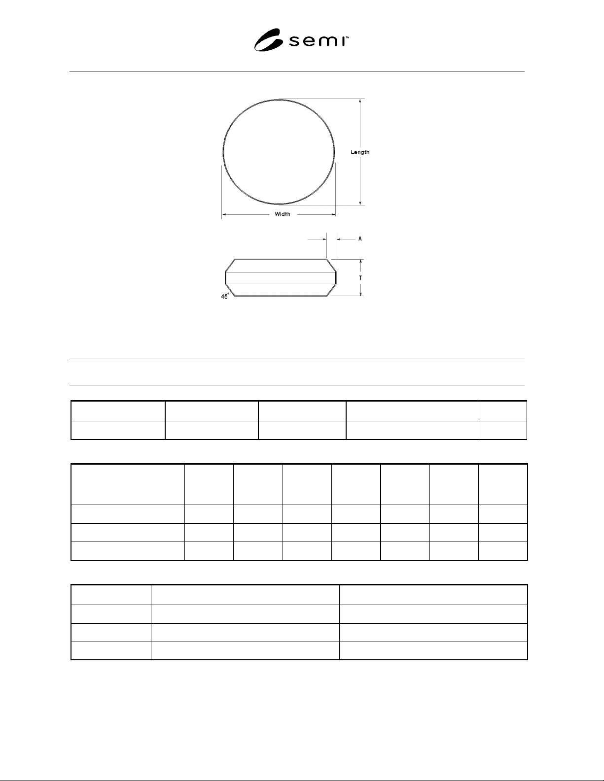
Table 2. Flatness Limits for Round Quartz Photomask Substrates
Table 3. Edge Criteria for Round Quartz Photomask Substrates
Table 4. Glass Substrate Defect Limits per Plate
Internal Defects in the Quality Area
OPAQUE SPOT BUBBLE TOTAL DEFECTS (per inch
2
) NOTES
ULTE Glass
≥ 2 µm ≥ 2 µm
0.05 1 & 2
Surface Defects in the Quality Area
RESIDUE
SCRATCH
SIZE
TOTAL
DEFECTS
SLEEK SIZE
TOTAL
DEFECTS
(per in.
2
)
OPAQUE
SPOT SIZE
TOTAL
DEFECTS
(per in.
2
)
FRONTSIDE ULTE Glass
None
≥ 1.0 mm
0
≥ 2 µm
0
≥ 2.0 µm
0
< 1.0 µm
No limit
1-2 µm
0.1
1-2.0 µm
0.1
BACKSIDE ULTE Glass
≥ 3.0 µm
None
≥ 3.0 µm
None
≥ 10 µm
0.3
Defects Outside the Quality Area
EDGE CHIPS Defect Limit Total Number
Radial Depth
≥ .030"
None
Peripheral Cord
≥ .030"
None
Other Shall be negotiated between vendor and supplier. Shall be negotiated between vendor and supplier.
NOTES:
1. The size of internal defects is defined as 1/2 (long axis + short axis).
2. This table is based on the assumption that defects < 2 µm will fall outside the focal depth of the lens system and should not print.
T
A
2.3 mm (.090") .10 mm (min.) - .6 mm (max.)
3.0 mm (.120") .10 mm (min.) - .6 mm (max.)
Chamfered Edge Criteria
SEMI P4-92 © SEMI 1983, 1999 5
Table 5. Specification for Diameter, Flat Depth, and Thickness for Round Substrates (proposed)
Nominal
Diameter
Diameter
(A) Min.
Diameter
(A) Max.
Flat Depth
(B) Min.
Flat Depth
(B) Max.
Nominal
Thickness (C)
Thickness
Min.
Thickness
Max.
Units
7 1/4" 183.75 184.55 88.52 88.65 3.81 3.69 3.94 mm
7 1/4" 7.234 7.266 3.485 3.490 0.150 0.145 0.155 in.
177.8 mm
Flatness Limits
10 µm TIR
5 µm TIR
3 µm TIR
152.4 mm
177.8 mm
SEMI P4-92 © SEMI 1983, 1999 6
APPENDIX 1
NOTE: This appendix was approved as an official part
of SEMI P4 by full letter ballot procedure.
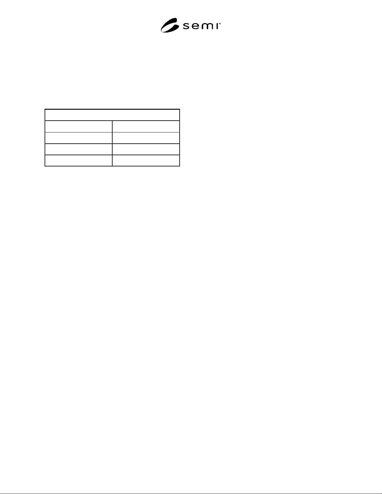
Hard Surface Photomask Glass Properties
Quartz Properties
Property
Ultra Low Thermal Expansion Ulte
Modulus of Elasticity
6.7-7.4 × 10
3
Kg/mm
2
Poisson' s Ratio 0.18-0.19
(1)
Specific Gravity 2.18-2.20 g/cm
3
Index of Refraction 1.46
NOTE: These properties are not absolute requirements. For
more specific information, contact your individual supplier.
NOTICE: These standards do not purport to address
safety issues, if any, associated with their use. It is the
responsibility of the user of these standards to establish
appropriate safety and health practices and determine
the applicability of regulatory limitations prior to use.
SEMI makes no warranties or representations as to the
suitability of the standards set forth herein for any
particular application. The determination of the
suitability of the standard is solely the responsibility of
the user. Users are cautioned to refer to manufacturer' s
instructions, product labels, product data sheets, and
other relevant literature respecting any materials
mentioned herein. These standards are subject to
change without notice.
The user' s attention is called to the possibility that
compliance with this standard may require use of
copyrighted material or of an invention covered by
patent rights. By publication of this standard, SEMI
takes no position respecting the validity of any patent
rights or copyrights asserted in connection with any
item mentioned in this standard. Users of this standard
are expressly advised that determination of any such
patent rights or copyrights, and the risk of infringement
of such rights, are entirely their own responsibility.
Copyright by SEMI® (Semiconductor Equipment and Materials
International), 3081 Zanker Road, San Jose, CA 95134. Reproduction o
f
the contents in whole or in part is forbidden without express written
consent of SEMI.