semi合集-English.pdf - 第5191页
SEMI M34-0299 © SEMI 1999 9 back sides of the wafer. The mean value on t h e backside of the wafer will typically be at least 10 microseconds for N-type m a terial and 3 m icroseconds for P-type material. These va lues c…
SEMI M34-0299 © SEMI 1999 8
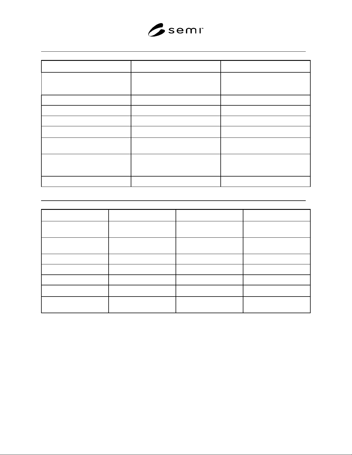
Table 2. Example SIMOX Wafer Surface Inspection Criteria
Criterion Allow Quantity Description
Slip 0.3 mm: NONE
0.1−0.3 mm: < 15 mm total
< 0.1 mm: OVERLOOK
6 mm edge exclusion
Scratch NONE 6 mm edge exclusion
Contamination NONE Backside
Stain < 5 spots < 0.05 cm
2
total area
Edge Chips/Cracks < 1.5 mm circumferential < 1.8 mm radial
combined length 1 × bright light
Pits and Dimples < 0.5 mm - 10/wafer
> 0.5 mm - NONE
1 × bright light
Haze Moderate haze - NONE
Heavy haze - NONE
Non-uniform haze - NONE
Light uniform haze is acceptable.
(Iterate between user and vendor.)
Foreign Matter (embedded particles) < 0.05/cm
2
< 3 embedded particles per 150 mm wafer
Table 3. SIMOX Electrical Parameters
Parameters Reference Value Method
Photoconductivity Lifetime
(Backside)
Section 8.1
> 1 msec.
microwave
Photoconductivity Lifetime
(Front side)
Section 8.1 TBD microwave
BOX Breakdown Section 8.2 > 5 MV/cm I-V
BOX Pinholes Section 8.3 < 0.2 cm
2
I-V
BOX Charge Section 8.4 < C-V
BOX Surface States Section 8.5
< 5 × 10
10
/cm
2
C-V
Doping Density
Sub, Surface
Section 8.6 TBD 4-point probe
8. Electrical Parameters
8.1 Photoconductivity Lifetime — This is measured by
creating an excess of carriers (typically by using a light
source) and measuring the slope of the decay curve.
Several pieces of commercial equipment are available
for this purpose. This requires that polysilicon is not
deposited on the backside, as is sometimes done for
gettering. Also, surface passivation may be needed for
lifetime measurements. Backside measurements
indicate the quality of the substrate and can be
performed by traditional methods. Frontside
measurements are more difficult and must be performed
using incident light which can be entirely absorbed
before reaching the underlying substrate.
8.1.1 Typically, the sample is placed on a micro-wave
wave guide post, forming part of a transmission line
circuit. The microwave reflection is determined by the
total conductivity of the sample and the conductivity is
modulated by an intense light pulse. When the light is
turned off, the microwave detects an exponential decay
in conductivity from which a decay constant is
determined. The photoconductivity lifetime is a result
of the recombination velocity at the surfaces, volume
recombination in the silicon layer, and any trapping.
Measurements are made independently on the front and

SEMI M34-0299 © SEMI 1999 9
back sides of the wafer. The mean value on the
backside of the wafer will typically be at least 10
microseconds for N-type material and 3 microseconds
for P-type material. These values correspond to about a
100 micron diffusion length (SPV value).
8.1.2 The relevance of photoconductivity lifetime to
the users requirement should be discussed. The use of
this measurement should be negotiated between
customer and vendor.
8.2 BOX Breakdown This parameter can be
measured with a buried oxide capacitor (BOX-CAP).
The buried oxide thickness and the intended application
will affect both the test procedure (such as capacitor
area and voltage criterion) and the allowable values of
measured parameters. These should be determined by
agreement between the user and vendor. Example
procedure and values for standard evaluation of 400 nm
thick buried oxide are given in the following
paragraphs.
8.2.1 Test Structure — Buried oxide capacitor (BOX-
CAP) having an area of 0.01 cm
2
for standard (400 nm)
BOX. The electrode material and thickness affect the
breakdown phenomena due to thermal effects, and so
should be included in the agreement between customer
and vendor.
8.2.2 Test Method: Staircase I-V Measurement —
Voltage is stepped in one-volt increments from zero to
400 volts, or until destructive breakdown is sensed.
Tests are done for both bias polarities. The test detects
the onset of high field conduction, as well as the point
of destructive or massive charge injection and trapping.
8.2.3 Typical Values
J
ox
< 10
-8
A/cm
2
at E
ox
= ± 2 MV/cm [onset of hi-E
regime]
E
ox
> 5 MV/cm at J
ox
= 0.01 A/cm
2
[break-
down/injection]
8.3 BOX Pinhole Density This parameter can be
measured with a buried oxide capacitor (BOX-CAP).
The buried oxide thickness and the intended application
will affect both the test procedure (such as capacitor
area and voltage criterion) and the allowable values of
measured parameters. These should be determined by
agreement between the user and vendor. Example
procedure and values for standard evaluation of 400 nm
thick buried oxide are given in the following
paragraphs.
8.3.1 Test Structure — Buried oxide capacitor having
an area equal to or greater than 0.05 cm
2
.
8.3.2 Test Method: Staircase I-V — Measurement
testing can be done for both Type I and Type II defects
where Type I defects are silicon pipes traversing the
buried oxide, and Type II defects are local regions of
thin buried oxide. If Type II defect density is sought,
capacitors are subjected to a series of 30 voltage steps
of 3.3 volts, with current monitored after each step,
using a failure criterion of 1 nA.
8.3.2.1 Arrays of at least 200 capacitors per wafer are
tested. Bias polarity of the voltage ramp is chosen so as
to accumulate the substrate portion of the capacitor
(positive for n-silicon, negative for p-silicon).
8.3.2.2 Type I defect density is determined using the
same test procedure, except that the failure current
criterion is 1 µΑ.
8.3.2.3 Any capacitor displaying the failure current or
more for voltages less than 100 volts is considered
defective. Defect density of either type is calculated
from the yield of good capacitors, (Y = 1 − # failed/#
tested), using Poisson statistics;
D = -1n (Y)/A,
where A is the total area of the capacitors tested.
8.3.2.4 For thin buried oxide (films less than 360 nm),
the voltage criteria above need to be adjusted to account
for the onset of high field conduction in defect-free
capacitors.
8.3.3 Values
D (Type I) < = 0.2 defects/cm
2
8.3.3.1 No standardized criterion for Type II defects
has been established.
8.4 Buried Oxide Charge This parameter can be
measured with a buried oxide capacitor (BOX-CAP).
The buried oxide thickness and the intended application
will affect both the test procedure (such as capacitor
area and voltage criterion) and the allowable values of
measured parameters. These should be determined by
agreement between the user and vendor. Example
procedure and values for standard evaluation of 400 nm
thick buried oxide are given in the following
paragraphs.
8.4.1 Test Structure — Buried oxide capacitor having
an area of 0.01 cm
2
.
8.4.2 Test Method — MOS high frequency C-V
measurement of a buried oxide capacitor normally
yields a flat band voltage less than one volt in
magnitude. For a previously untested 400 nm film, this
implies an effective fixed charge density of less than 5
Ξ 10
10
charges/cm
2
.
8.4.3 Values
Qf/q < = 5 × 10
10
/cm
2

SEMI M34-0299 © SEMI 1999 10
8.5 Buried Oxide Fast Interfaces State Density This
parameter can be measured with a buried oxide
capacitor (BOX-CAP). The buried oxide thickness and
the intended application will affect both the test
procedure (such as capacitor area and voltage criterion)
and the allowable values of measured parameters.
These should be determined by agreement between the
user and vendor. Example procedure and values for
standard evaluation of 400 nm thick buried oxide are
given in the following paragraphs.
8.5.1 Test Structure — Buried oxide capacitor having
an area of 0.01 cm
2
.
8.5.2 Test Method — High-Low Frequency MOS C-V.
If care is taken in their fabrication to minimize oxide
surface damage and contamination during silicon
etching, good quality quasi-static MOS C-V curves can
be measured on BOX-CAP' s. From comparison of high
and low frequency C-V curves, midgap interface state
density can be determined exactly as for normal MOS
capacitors.
8.5.3 Values
Dit (0) < = 5 × 10
10
states/ /cm
2
-eV
8.6 Doping Density in the SIMOX Layer
8.6.1 Test Structure — The untreated SIMOX wafer.
Substrate: Buried oxide capacitor, area = 0.01 cm
2
8.6.2 Test Method — Spreading Resistance Probing
(SRP) offers a way of determining the resistance profile
in the Si layer as a function of distance from the top
surface. The carrier concentration can be calculated
directly from this data.
8.6.2.1 The four point probe method of SIMS can also
be used. The four point probe test is liable to punch
through and should be considered a destructive test as is
SIMS. SIMS will allow for an understanding of
compensation effects, if any.
8.6.3 Values The acceptable dopant values are to be
determined by agreement between the user and vendor.
8.7 Doping Density in the Substrate
8.7.1 Test Structure A buried oxide capacitor
(BOX-CAP) area = 0.01 cm
2
.
8.7.2 Test Method The electrically active dopant
concentration in the substrate immediately beneath the
buried oxide can be determined from the standard
analysis of high frequency MOS C-V curves measured
on BOX-CAPs, dependent on oxide charge and
interface properties.
Values — The acceptable dopant values are to be
determined by agreement between the user and vendor.
9. Packing and Marking
9.1 Special packing requirements shall be subject to
agreement between the user and supplier. Otherwise, all
wafers shall be handled, inspected, and packed in such
a manner as to avoid chipping, scratches, and
contamination and in accordance with the best industry
practices to provide ample protection against damage
during shipment.
9.2 The wafer supplied under these specifications shall
be identified by appropriately labeling the outside of
each box or other container, and each subdivision
thereof, in which it may reasonably be expected that the
wafers will be stored prior to further processing.
Identification marks, codes, symbols and content shall
be agreed upon between user and supplier.
NOTICE: These guidelines do not purport to address
all of the safety issues associated with their use. It is the
responsibility of the users of these guidelines to
establish appropriate safety and health practices and
determine the applicability of regulatory limitations
prior to use. SEMI makes no warranties or
representations as to the suitability of the guidelines set
forth herein for any particular application. The
determination of the suitability of these guidelines is
solely the responsibility of the user. Users are cautioned
to refer to manufacturer' s instructions, product labels,
product data sheets, and other relevant literature
respecting any materials mentioned herein. These
guidelines are subject to change without notice.
The user' s attention is called to the possibility that
compliance with this standard may require use of
copyrighted material or of an invention covered by
patent rights. By publication of this standard, SEMI
takes no position respecting the validity of any patent
rights or copyrights asserted in connection with any
item mentioned in this standard. Users of this standard
are expressly advised that determination of any such
patent rights or copyrights, and the risk of infringement
of such rights, are entirely their own responsibility.
Copyright by SEMI® (Semiconductor Equipment and Materials
International), 3081 Zanker Road, San Jose, CA 95134. Reproduction o
f
the contents in whole or in part is forbidden without express written
consent of SEMI.