semi合集-English.pdf - 第7449页
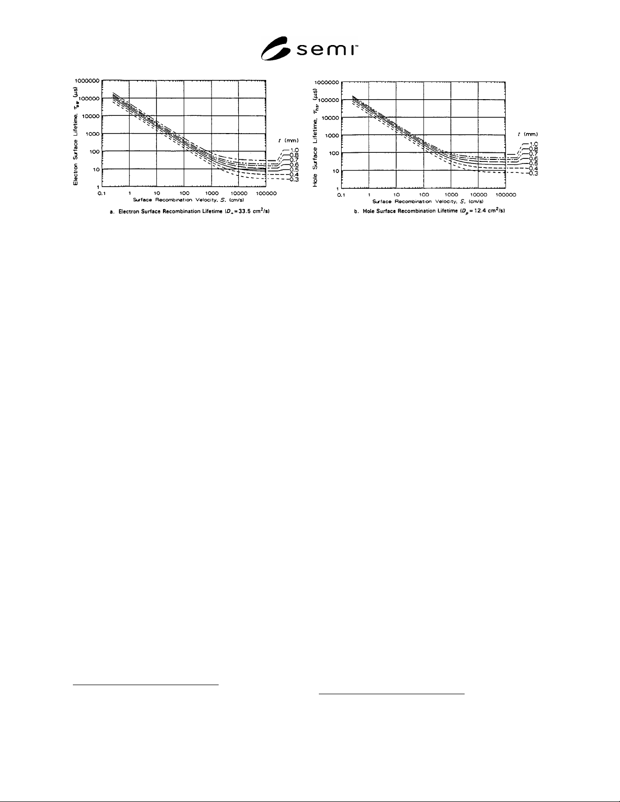
SEMI MF1535-1104 © SEMI 2004 7 Note: The maximum bulk recombination lifetime that can b e a ccurately measured is about 1/10 of the surface lif etime. Figure 2 Surface Recombination Lifetime as a Function of Surfa ce Rec…

SEMI MF1535-1104 © SEMI 2004 6
9.3 The chemicals used for etching and for some
surface passivating solutions are potentially harmful
and must be handled in an acid exhaust fume hood,
with proper protective gear including safety goggles,
and with utmost care at all times. Warning:
Hydrofluoric acid solutions are particularly hazardous.
HF solutions should not be used by anyone who is not
familiar with the specific preventive measures and first
aid treatments given in the appropriate Material Safety
Data Sheet.
10 Sampling
10.1 If the test method is not used on a 100%
inspection basis, sampling procedures shall be agreed
upon by the parties to the test.
10.2 If sampling by lot is required, the determination
of what constitutes a lot and the procedures for
sampling and the procedures for sampling by lot shall
be agreed upon by the parties to the test.
10.3 Because the concentration of recombination
centers in a wafer may be non-uniform, it is desirable to
determine the recombination lifetime at various points
across the wafer surface. The point density and
location of points measured shall be agreed upon by the
parties to the test.
11 Test Specimen Preparation
11.1 The required test specimen preparation depends
on both the surface condition of the test specimen and
the expected magnitude of the bulk recombination
lifetime,
b
, to be measured.
11.2 No test specimen preparation is required if the
value of
b
is no greater than one-tenth of the surface
recombination lifetime,
s
. The surface recombination
lifetime is composed of two terms, a diffusion term,
diff
, which accounts for the diffusion of carriers to the
surface, and a surface recombination term,
sr
, which
accounts for the recombination at the surface. The
surface recombination lifetime may be computed from
the following approximate relation:
10
S
L
D
L
srdiffs
2
2
2
(1)
where:
D = minority carrier diffusion coefficient, in cm
2
/s,
L = wafer thickness, in cm, and
10 Horányi, T. S., Pavelka, T., and Tüttô, P., “In Situ Bulk Lifetime
Measurement on Silicon with Chemically Passivated Surface,”
Applied Surface Science, Vol 63, 1993, pp. 306–311.
S = surface recombination velocity, in cm/s, assumed
equal on both surfaces.
Electron and hole surface recombination lifetimes are
shown in Figure 2 as a function of surface
recombination for wafers with different thickness
11
(Note 4).
NOTE 4: If S is very large (>10
4
cm/s) excess carriers
recombine immediately on striking the surface so the surface
recombination lifetime is dominated by
diff
. A well polished
surface has a surface recombination velocity of ~10
4
cm/s
10
while for an abraded (lapped) surface the surface
recombination velocity is even larger (~10
7
cm/s, the carrier
saturation velocity). In such cases, the maximum bulk
recombination lifetime that can be measured to 10% accuracy
in wafers of standard thickness is about 1 s for p-type wafers
and about 2 s for n-type wafers. In spite of this limitation of
accurate determination of the bulk recombination lifetime, it
is possible to detect relative variations of bulk recombination
lifetime on unpassivated polished wafers that have bulk
recombination lifetime as large as 0.5 to 1 ms provided that
the following conditions are met:
(1) the diffusion coefficient and surface recombination
velocity are uniform over the wafer, and
(2) the microwave system is sensitive enough to resolve
measured lifetimes which differ by 1%.
Under these same conditions, relative measurements can be
made on lapped wafers with bulk recombination lifetimes up
to about 100 s. In this case, it may be necessary to etch the
surfaces in bright etching solution (see Section 8.5) for about
1 min in order to obtain sufficient uniformity of the surface
recombination velocity.
11.3 If bulk recombination lifetimes larger than about
0.1
s
are to be measured, the wafer surfaces must be
passivated by one of the following methods (Note 5) to
obtain accurate measurements.
11.3.1 Oxidation — Bulk recombination lifetimes up
to about 1 ms can be measured on wafers 0.5 mm
thick that have a very high quality (dry) thermal oxide
(D
it
< 10
10
/cm
2
·eV) (Note 6). Ensure that the oxidation
conditions are such that significant numbers of oxide
precipitates do not form during the oxidation cycle (see
Section 3.2.2). For measurement of lifetimes between
about 1 ms and 10 ms, strip the oxide in dilute HF (see
Section 8.6) and make the measurement within 15 min.
11 For these estimates, the diffusion coefficients were assumed to be
constant at the following limiting values: D
n
= 33.5 cm
2
/s and
D
p
= 12.4 cm
2
/s. These values are somewhat smaller than the limiting
values given in the 1993 edition of DIN 50 440, Part 1.
SEMI MF1535-1104 © SEMI 2004 7
Note: The maximum bulk recombination lifetime that can be accurately measured is about 1/10 of the surface lifetime.
Figure 2
Surface Recombination Lifetime as a Function of Surface Recombination Velocity for Constant Diffusion
Coefficient and Selected Values of Wafer Thickness
11.3.2 Immersion in Passivating Solution — To
measure bulk recombination lifetimes up to ~1 ms on a
bare polished wafer 0.5 mm thick, first pretreat the
wafer in iodine-ethanol passivating solution (see
Section 8.4) or an alternative passivating solution.
Then enclose the wafer in a small plastic bag or other
fixture containing enough of the passivating solution to
coat the surface with a thin film while the measurement
is being made. Ensure that the passivation technique
results in stable and repeatable measurements before
proceeding with the test (see Section 3.2.1).
11.3.2.1 If the wafer is oxidized, passivate it with
iodine-ethanol, an alternative passivating solution, after
first removing the oxide by etching in dilute HF
solution for a time that depends on oxide thickness;
etch times range from about 30 s for thin oxide (<5 nm)
to about 10 min for thick oxide (~200 nm).
11.3.2.2 Again, ensure that the passivation technique
results in stable and repeatable measurements before
proceeding with the test (see Section 3.2.1).
NOTE 5: Polished surfaces that have been oxidized or
passivated with certain chemical solutions have much reduced
surface recombination velocity. For example, carefully
prepared thermally oxidized silicon surfaces have surface
recombination velocity as low as 1.5 to 2.5 cm/s while the
surface recombination velocity can be as low as 0.25 cm/s
following stripping of the oxide in hydrofluoric acid.
12
This
reference also outlines a procedure for determining surface
recombination velocity. Immersion in the iodine-ethanol
passivating solution (Section 8.4) has been shown to reduce
surface recombination velocity of a chemically polished,
oxide-free silicon wafer to 10 cm/s.
10
12 Yablonovitch, E., Allara, D. L., Chang, C. C., Gmitter, T., and
Bright, T. B., “Unusually Low Surface-Recombination Velocity on
Silicon and Germanium Surfaces,” Phys. Rev. Lett. 57, 249–252
(1986).
NOTE 6: The density of interface trapped charge (D
it
) can be
measured by a variety of techniques described in the
literature;
13
however, none of these techniques has been
standardized.
12 Procedure
NOTE 7: The following procedures are given in sufficient
detail for manual data collection and analysis. However it is
strongly recommended that instrument setup, data collection,
and analysis be carried out using computer-controlled
equipment, with data storage and display capabilities. In such
cases, the procedures and algorithms employed must be
equivalent to those given in this section.
12.1 If they are not known, determine the conductivity
type in accordance with SEMI MF42, the center-point
wafer thickness in accordance with SEMI MF533 or
SEMI MF1530, and the center-point resistivity in
accordance with SEMI MF84 or SEMI MF673.
Convert the resistivity to the density of the majority
carriers (n
maj
, in carriers/cm
3
) in accordance with SEMI
MF723. Record these data together with the nominal
diameter and the condition (polished, etched, lapped,
as-cut, etc.) of the front and back surfaces.
12.2 Record the temperature of the room, or if the
stage is temperature-controlled, the temperature of the
stage surface.
12.3 Load the wafer onto the stage so that the light
pulse will strike the desired region.
12.4 Switch on the pulsed laser light source (see
Section 7.1).
12.5 Adjust the intensity so that the injection level,
,
is at the specified value. If an injection level has not
been specified, set it to 100. If it is not adjusted
13 See, for example, Schroder, D. K., Semiconductor Material and
Device Characterization (John Wiley & Sons, New York, 1990) pp.
267–286.
SEMI MF1535-1104 © SEMI 2004 8
automatically by the apparatus, set the injection level as
follows:
12.5.1 If the test specimen is oxidized and the
thickness of the oxide layer is not known, measure or
estimate it, using a method acceptable to the parties to
the test. Record the thickness.
12.5.2 Determine and record the fraction of the
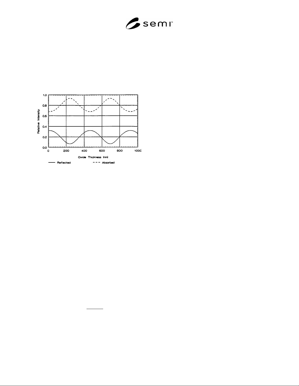
incident light that penetrates the oxide and is absorbed
by the specimen from the dashed curve in Figure 3.
Note: For these calculations the wavelength of the incident
radiation, , is assumed to be 905 nm, the index of refraction
of silicon is taken as 3.610, and the index of refraction of SiO
2
is taken as 1.462. Maximum absorption occurs at an oxide
thickness d = (2n + 1)/4 while minimum absorption occurs
at an oxide thickness d = n/2, when n = 0, 1, 2, etc.
Therefore, if the wavelength of the incident radiation,
1
,
differs from 905 nm, these curves can be used by determining
the relative intensity for an effective oxide thickness d
0
= 905
d
1
/
1
where d
1
is the actual thickness of the oxide.
Figure 3
Fraction of Incident Radiation Reflected from (solid
line) or Absorbed in (dashed line) a Silicon Wafer
Covered with a Silicon Dioxide (SiO
2
) Layer
between 0 and 1
m Thick
12.5.3 Adjust the light source intensity so that the
photon density absorbed in the silicon during the pulse,
, is equal to
n
maj
, where
is the desired injection
level and n
maj
is the density of majority carriers in the
wafer as determined in Section 12.1. The photon
density,
, in photons/cm
3
, is given by:
L
tf
p
t
I
0
d
(2)
where:
f
=
the fraction absorbed found from Figure 3 (see
Section 12.5.2),
I
=
the intensity of the incident light, in photons/cm
2
·s,
t
p
=
the length of the light pulse, in s, and
L
=
wafer thickness, in cm.
12.6 Turn on the microwave power source and view
the photoconductivity decay on the display unit. Adjust
the time and voltage scales so as to display the desired
portion of the decay signal. In the absence of
indications to the contrary, observe the decay signal
from 45 to 5% of the peak voltage.
12.7 Determine that the decay is exponential over the
desired range. Determine the time constant by fitting
an exponential curve to the voltage, V, as a function of
time, t, or (for manual data collection) a straight line to
the curve of lnV as a function of t.
12.8 Record this time constant as the recombination
lifetime.
12.9 If desired, move the wafer position and repeat
Sections 12.6 through 12.8 as required to obtain a wafer
map, noting the point spacing and pattern together with
the radius of the mapped area.
12.10 Alternatively, if desired, repeat Sections 12.2
and 12.6 through 12.8 at the same location for different
temperatures or repeat Sections 12.5 through 12.8 at the
same location for different values of injection level.
13 Report
13.1 Report the following information:
13.1.1 Date and location of the test,
13.1.2 Operator,
13.1.3 Instrument type, model number, and, if
computer controlled, software version,
13.1.4 Wafer description including any identification
markings, center-point resistivity, center-point
thickness, conductivity type, surface condition (front
and back), and nominal diameter,
13.1.5 Portion of the decay signal from which the time
constant was determined,
13.1.6 Injection level,
, as established in Section 12.5,
13.1.7 Surface passivation procedure used (see Section
11), and
13.1.8 Carrier recombination lifetime,
, in s.
13.2 If measurements were made at several injection
levels, report
for each value of
.