semi合集-English.pdf - 第7487页
SEMI MF1630-0704 © SEMI 2004 7 RELATED INFORMATION 1 DERIVATION OF FACTORS USED IN CALCULATING CONCENTRATIONS AND DENSITIES OF ELEMENTS IN SILICON NOTICE: This relat ed informat ion is not an offici al part of SEM I MF16…
SEMI MF1630-0704 © SEMI 2004 6
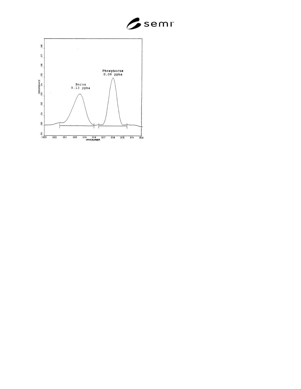
Figure 3
Boron and Phosphorus Region Expanded and
Baseline Corrected
14 Report
14.1 Report the following information:
14.1.1 The instrument used, the operator, and the date
of the measurements,
14.1.2 Identification of specimens,
14.1.3 The results of the audit reference specimen on a
control chart or other suitable form,
14.2 For each sample specimen report the following
information:
14.2.1 The concentration of each impurity/dopant or the
detection limit if no peaks can be identified,
14.2.2 Sample thickness,
14.2.3 The FWHM for each absorption peak,
14.2.4 The apodization function used, and
14.2.5 The amount of zero-fills and resulting number of
data points/cm
−1
.
15 Precision
15.1 A within-laboratory precision was determined by
measurement of boron and phosphorus in a reference
specimen by multiple operators over a period of one
year. The relative precision was determined to be 8.5%
and 9.7% for boron and phosphorus, respectively, at
nominal concentrations of 0.095 and 0.072 ppba.
16 Bias
16.1 The bias of this test method is not known but
believed to be within ± 10% of an accepted reference
value.
17 Keywords
17.1 analysis of silicon; determination of dopants;
determination of impurities; electrically active
impurities; Fourier transform infrared; impurities;
silicon.

SEMI MF1630-0704 © SEMI 2004 7
RELATED INFORMATION 1
DERIVATION OF FACTORS USED IN CALCULATING
CONCENTRATIONS AND DENSITIES OF ELEMENTS IN SILICON
NOTICE: This related information is not an official part of SEMI MF1630. It was developed as non-mandatory
information in ASTM during the initial development of the document in 1994-5. This related information was
approved for publication by SEMI by full letter ballot procedures on March 14, 2004.
R1-1 The factors shown in Table 1 resulted from
several years of corrections and modifications but are
ultimately based on resistivity measurements on silicon
samples. The dopant density, or the concentration of
impurities for this test method, is directly obtained
from the conversion Tables found in SEMI MF723.
R1-2 Baber’s
5
calibration factors published in 1980,
were the starting point for the current factors.
Corrections or modifications, or both, to his published
data follow in this discussion.
R1-2.1 Baber’s LTFT-IR study utilized the conversion
relations reported by Irvin
7
in 1962, relating resistivity
and impurity concentrations. Currently, the conversion
tables given in SEMI MF723 are believed to be more
reliable. Corrections to Baber’s factors were made to
reflect these new conversion tables.
R1-2.2 The factors of Baber relate peak heights of the
absorption bands to concentrations. Peak heights are
extremely sensitive to several FT-IR parameters. The
phosphorus band at 316.0 cm
−1
and the arsenic band at
382.0 cm
−1
are very narrow, about 0.25 cm
−1
, and thus
the peak heights of these bands vary greatly with
nominal resolution, type of apodization, degree of zero-
filling, and mechanical strain on the sample. The boron
absorption at 319.6 cm
−1
band used in this test method
is actually a composite of four separate boron
absorption bands. The variability of the measurement
of the absorption bands is reduced considerably when
peak areas are used instead of peak heights. The use of
peak areas is common in the field and their use is
specified in this test method.
R1-2.3 Further minor modifications have been made
over the in the period from about 1985 to about 1995 in
several laboratories that use LTFT-IR spectrometers for
determination of electrically active impurities.
R1-2.3.1 Studies with and without the white light on
the silicon samples, covering a wide range of
concentrations, are valuable as tools to check for
consistency of the boron and phosphorus factors, which
are indeed the most common impurities. With the
absence of white light, the LTFT-IR method shows
7 Irvin, J. C., “Resistivity of Bulk Silicon Diffused Layers in
Silicon,” Bell System Tech. J. 41, 387–410 (1962).
only the net carrier absorption bands at an intensity
proportional to the excess majority carrier
concentration. These data along with the total
impurities obtained with white light on the samples
permitted minor adjustments to the boron or
phosphorus factors, or both.
R1-2.3.2 Silicon samples whose resistivity has been
carefully determined have been measured by LTFT-IR
spectroscopy, and the results used to confirm or slightly
modify the calibration factors.
R1-3 In 1990, a pilot study was conducted in which ten
silicon samples were examined at four different
laboratories by either LTFT-IR or photoluminescence,
or both, and the results compared. Even though each
laboratory used their own factors and modifications of
this test method for determination of impurity
concentrations, the data for boron and phosphorus all
agreed to within ± 20% of the average value. The
factors given in this test method are approximately
equal to the average values from that study.
R1-4 In summary, the factors given in Table 1 are a
result of continued refinement as more and better
measurements have been made. However, they
ultimately correspond to the resistivity measurements
and the conversion to dopant (impurity) concentrations
as given in SEMI MF723. The factors for boron and
phosphorus have the highest degree of certainty since
these two elements are the most commonly measured
and are therefore studied the most. The factors for the
other elements, especially aluminum, antimony,
gallium, and indium, should be considered only
approximations and used only to estimate their
concentrations in silicon.

SEMI MF1630-0704 © SEMI 2004 8
NOTICE: SEMI makes no warranties or
representations as to the suitability of the standards
set forth herein for any particular application. The
determination of the suitability of the standard is
solely the responsibility of the user. Users are
cautioned to refer to manufacturer' s instructions,
product labels, product data sheets, and other
relevant literature, respecting any materials or
equipment mentioned herein. These standards are
subject to change without notice.
By publication of this standard, Semiconductor
Equipment and Materials International (SEMI)
takes no position respecting the validity of any
patent rights or copyrights asserted in connection
with any items mentioned in this standard. Users
of this standard are expressly advised that
determination of any such patent rights or
copyrights, and the risk of infringement of such
rights are entirely their own responsibility.
Copyright by SEMI® (Semiconductor Equipment and Materials
International), 3081 Zanker Road, San Jose, CA 95134. Reproduction o
f
the contents in whole or in part is forbidden without express written
consent of SEMI.