semi合集-English.pdf - 第2597页
SEMI E91-0600 © SEMI 1999 , 2000 2 4.8 job — a lot, proces sed with a s i n gle process program o n PSEM equ ip m ent. 4.9 l oad — move material to the p r o b ing or marking location from the cassette. 4.10 lot — a g ro…

SEMI E91-0600 © SEMI 1999, 20001
SEMI E91-0600
SPECIFICATION FOR PROBER SPECIFIC EQUIPMENT MODEL
(PSEM)
This specification was technically approved by the Global Information & Control Committee and is the direct
responsibility of the Japanese Communications Committee. Current edition approved by the Japanese
Regional Standards Committee on January 14, 2000. Initially available at www.semi.org March 2000; to be
published June 2000. Originally published September 1999.
1 Purpose
1.1 This document establishes a S pecific Equipment
Model for prober equipment (PSEM). The PSEM
consists of equipment characteristics and behaviors that
apply to this class of equipment and are required to be
implemented in addition to the fundamental
requirements and additional capabilities specified in
SEMI E30 (GEM). The intent of this document is to
facilitate the integration of prober equipment into an
automated semiconductor factory. This document
accomplishes this by defining an operational model for
prober equipment as viewed by a factory automation
controller. This definition provides a standard host
interface and equipment operational behavior.
2 Scope
2.1 The scope of this document is limited to the
definition of prober equipment behavior as perceived
by a Semiconductor Equipment Communications
Standard (SECS-II) (SEMI E5) host that complies with
GEM. The document defines the view of the equipment
through the SECS communications link, but does not
define the internal operation of the equipment. It
includes a specific processing state model as the basis
for the behavior of all equipment of this class.
2.2 This document requires that th e GEM fundamental
requirements and applicable additional capabilities have
been implemented on the prober equipment. This
document expands GEM Standard requirements and
capabilities in the areas of the processing state model,
collection events, remote commands, data item
variables and process program management, and adds
Prober Job state model to GEM Standard requirements
and capabilities. This document does not include the
definition of the treatment of Multiple Stage.
2.3 This document applies to the class of prober
equipment in which the wafer is unloaded from the
same slot in the same carrier which loaded the wafer
after processing.
2.4 This standard does not purport to address safety
issues, if any, associated with its use. It is the
responsibility of the users of this standard to establish
appropriate safety and health practices and determine
the applicability of regulatory limitations prior to use.
3 Referenced Standards
3.1 SEMI Standards
SEMI E5 — SEMI Equipment Communications
Standard 2 Message Content (SECS-II)
SEMI E30 — Generic Model for Communications and
Control of Manufacturing Equipment (GEM)
SEMI M20 ― Specification for Establishing a Wafer
Coordinate System
SEMI M21 ― Specification for Assigning Addresses to
Rectangular Elements in a Cartesian Array
3.2 Other Documents
Harel, D., “Statechart: A Visual Formalism for
Complex Systems”, Science of Computer Programming
8 (1987) 231-274.
1
NOTE 1: As listed or revised, all documents cited shall be the
latest publications of adopted standards.
4 Terminology
4.1 alignment — a procedure in which a coordinate
system is established on a substrate.
4.2 bin — categorized data of die as a result of
measurement.
4.3 cassette — a physical object containing one or
more substrate locations (see slot). For example, a
SEMI standard cassette is a carrier with 25 substrate
slot locations.
4.4 die — 1. A field sub-unit. 2. An area of substrate
that contains the device being manufactured.
4.5 execution area — the area from which a current
copy of the process program instructions are executed.
4.6 inker — a resource of the prober. The
electromechanical units to put ink mark on die.
4.7 instruction data — the Result Data to refer on the
inspection process.
1 Elsevier Science, P.O. Box 945, New York, NY 10159-0945,
http://www.elsevier.nl/homepage/browse.htt
SEMI E91-0600 © SEMI 1999, 2000 2
4.8 job — a lot, processed with a s ingle process
program on PSEM equipment.
4.9 load — move material to the p robing or marking
location from the cassette.
4.10 lot — a group of one or more s ubstrates of the
same type (e.g., wafers, masks, CDs).
4.11 map — a list of coordinate positions of die on a
substrate. MAP is defined in accordance with SEMI
M21 in this document.
4.12 map data — the categorized d ata of die as a
result of measurement associated with coordinates.
Map data also have an information that identifies origin
die.
4.13 marking — the process of the prober that making
an ink mark on a die using the inker.
4.14 material — 1. The basic unit o f process,
physically a cassette or some cassettes. 2. A lot.
4.15 measurement — making a test , contacting the
probe card and the die. The tester sends to the prober a
categorized data as a result of test.
4.16 probe card — the electromech anical interface
necessary to enable temporary electrical contact
between the substrate to be tested and the tester
resource. May consist of multiple components.
4.17 re-inspection — a process whe re the same
substrate is tested again by using the inspected map
data.
4.18 slot — a physical location with in a cassette
capable of containing a substrate. (Also referred to as a
carrier location).
4.19 state — 1. A static set of cond itions. If the
conditions are met, the state is current (SEMI E30). 2.
A state reacts predictably to specific stimuli.
4.20 substrate — 1. The basic unit of material,
processed by PSEM equipment such as wafers.
4.21 testing equipment — an equipment class
generally consisting of integrated mechanisms and
controls for performing electrical tests of packaged
devices and or wafer die during the manufacturing
process.
4.22 unload — remove materials to the cassette slots
from the probing or marking location.
4.23 wafer end — the end of measuring process of a
wafer.
5 State Model
5.1 The purpose is to define the eq uipment-specific
processing state model and Prober Job state models
necessary to portray the expected operational states of
the equipment to enable host tracking and control in
place of a local operator.
5.1.1 The processing state models in this document are
required for implementing an PSEM-compliant prober,
in addition to the required state models in SEMI E30. A
state model consists of a state model diagram, state
definitions, and a state transitions’ table. A state model
represents the host’s view of the prober, but not
necessarily the actual prober operations. All PSEM
state model transitions shall be mapped sequentially
into the actual equipment events that satisfy the
requirements of those transitions. In certain
implementations, the prober may enter a state and has
already satisfied all of the conditions required by the
PSEM state model for transition to another state. In this
situation, the prober makes the required transition
without any additional actions.
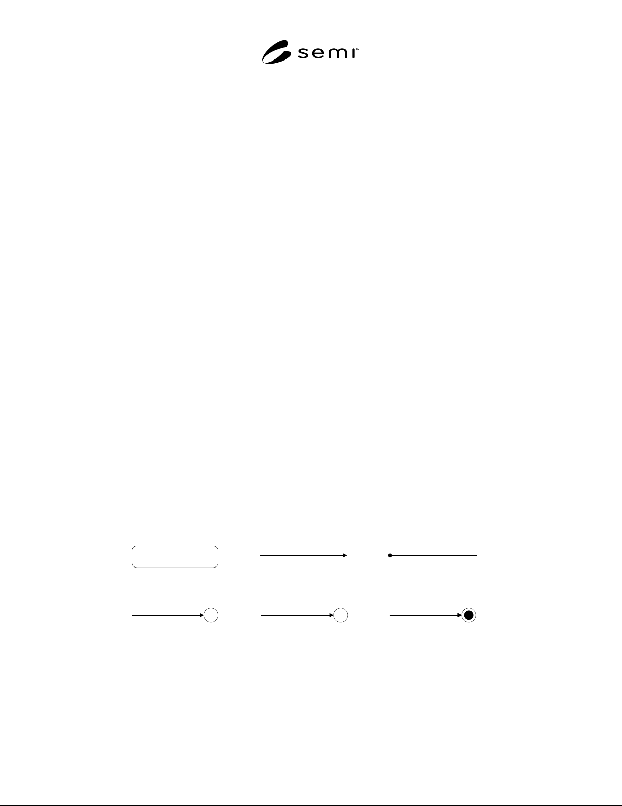
5.1.1.1 Various symbols used in a state diagram are
described in Figure 1.
a) State
b) Transition
c) Default Entry Point
H
d) History
C
e) Conditional Selector
f) Terminator
Figure 1
Various Symbols Used in a State Diagram
SEMI E91-0600 © SEMI 1999, 20003
5.1.2 Some equipment may need to include additional
states. However, any additional states must not change
the PSEM-defined state transitions. All expected
transitions between PSEM states must occur.
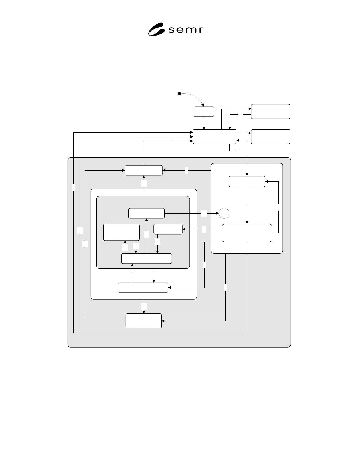
5.2 PSEM Processing State Model
5.2.1 Purpose
5.2.1.1 The purpose of the PSEM Processing State
Model is to make an accurate model for the behavior of
the PSEM prober from Processing State Model defined
in SEMI E30.
5.2.2 PSEM Processing State Model Diagram
INIT
IDLE with
Alarms
IDLE
EXECUTING
(PROBING)
MAINTENANCE
ABORTING
CHECKING
PAUSED
SETTING UP
PAUSING
PAUSED
ALARM PAUSED
STOPPING
2
3
4
7
8
9
C
10
11
12
6
21
13
18
17
16
19
15
14
20
23
24
25
26
PROCESS PAUSE
PAUSE
PROCESSING ACTIVE
PROCESS
SETTING UP
22
5
1
Figure 2
PSEM Processing State Model Diagram