semi合集-English.pdf - 第5186页
SEMI M34-0299 © SEMI 1999 4 type of material. The Secco Etch, as desc ribed, creates etch pits that appear as dark ci rcles roughly 50 nm in diameter, and pictures shou ld be taken at 250 0X to 20,000X m agnification in …

SEMI M34-0299 © SEMI 1999 3
7.1.2 Spectroscopic Ellipsometry Measurement — In
this measurement, white light from a xenon arc lamp
passes through a polarizing rotating filter and
illuminates the sample site under study; reflected light
passes through an analyzer to a monochromator and
photomultiplier detector. For each wavelength,
reflectivity oscillates with polarizer rotation; the
magnitude and phase of reflectivity changes are
measured to determine ellipsometric angles, δ and ψ.
The two measured spectra are fit by successive
approximation to allow determination of the silicon and
oxide layer thickness and oxide composition.
Ellipsometry measurements are only specified for the
annealed SIMOX wafers. For spectroscopic
ellipsometry, the choice of instrument and associated
model and fitting parameters affect the confidence-of-
fit, so they should be taken into account in the
user/supplier agreement. For example, with the SOPRA
SE system, the goodness-of-fit error estimator shall be
less than 0.025 for accurate structural models.
7.1.3 Optical Reflectance Measurements — In this
measurement, light from a xenon arc lamp passes
through a grating monochromator and illuminates the
sample site under study; reflected light is gathered by
an intrinsic silicon detector. Specular reflectivity is
plotted as a function of wavelength from 0.4 micron to
1.1 micron. The analysis proceeds by making
successively better approximations to the oxygen
content, index of refraction, and absorption of each
layer until an acceptable fit is achieved. Measurements
are made with a reflectance mode optical
interferometer.
7.1.4 Optical Model Fitting and Correlation — There
are slight, systematic differences between layer
thickness measured by reflectance and by spectroscopic
ellipsometry (SE). Because of this, user and supplier
should specify the actual measurement method to be
used. The two methods offer results which are
reproducible and well-correlated with each other over a
wide range of conditions. If both measurement
techniques are used, it is recommended that the
reflectance system measurements be calibrated to fit the
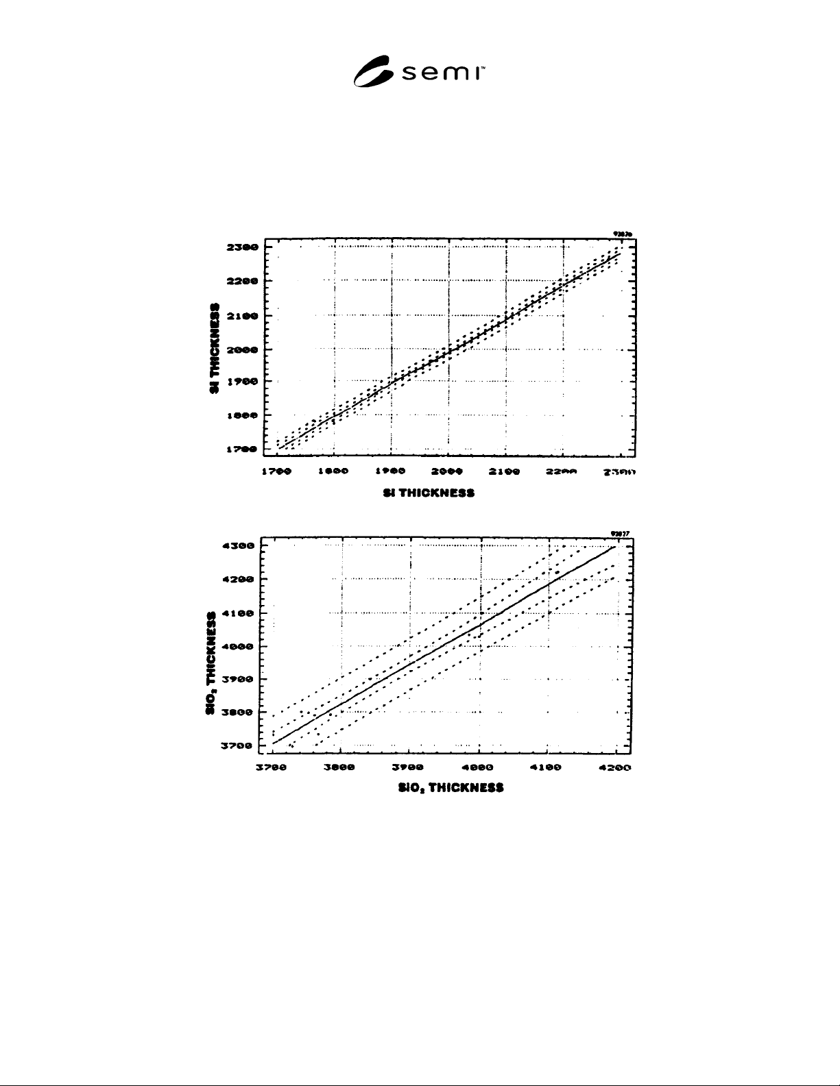
results of the SE. Figure 2 shows conversion curves for
top silicon and oxide layer thickness measurements
made with the two measurement techniques.
7.1.5 Top Silicon Layer Thickness — See Section
7.1.4 on correlation of reflectance and spectroscopic
ellipsometry (SE) measurements. Optical measure-
ments will be made on five wafer sites as shown in
Figure 1. Spectra for each site will be fit independently
with both the top silicon and oxide layer thickness as
adjustable parameters. Both the mean thickness and the
uniformity should be specified. Depending on the type
of SIMOX wafer being specified, the mean thickness of
the top silicon layer will be from 50 nm to 500 nm.
Following is an example specification: Mean top silicon
layer thickness for the five sites will be 215 ± 10 nm
with acceptable goodness-of-fit at all five sites. Top
silicon non-uniformity will be less than ± 5 nm.
7.1.6 Buried Oxide Layer Thickness — See Section
7.1.4 on correlation of reflectance and spectroscopic
ellipsometry (SE) measurements. Optical measure-
ments will be made on five wafer sites as shown in
Figure 1. Spectra for each site will be fit independently
with both the top silicon and the buried oxide layer
thickness as adjustable parameters. Both the mean
thickness and the uniformity should be specified.
Depending on the type of SIMOX wafer being
specified, the mean thickness of the buried oxide layer
is from 50 nm to 500 nm. Following is an example
specification: Mean buried oxide layer thickness for the
five sites will be 380 nm ± 20 nm with acceptable
goodness-of-fit at all five sites. Buried oxide uniformity
will be less than ± 10 nm.
7.2 Crystallographic Defect Measurements - Test
Methods — The evaluation of threading dislocation
density in the top SI layer will be made by destructive
chemical etching and microscopic etch pit density
measurements. The appropriate evaluation procedure
for given SIMOX wafer, which depends on the
threading dislocation density and the thickness of top Si
and buried oxide layers, will be determined by the
agreement between user and supplier.
7.2.1 Optionally, other crystallographic defects which
may be formed in the top Si layer of SIMOX wafers,
such as oxide precipitates or micro stacking faults,
silicon crystal defects induced by surface particles prior
to epi growth when epi is used to increase the thickness
of the top silicon. A sampling plan should be
established based on experience with the supplier.
7.2.2 Following are examples of the evaluation of
threading dislocations in two kinds of SIMOX wafers:
7.2.2.1 Example 1. Threading dislocation evaluation in
SIMOX wafers with 200 nm thick top Si layer and 400
nm thick buried oxide: Samples are handled with plastic
tweezers throughout the etching procedure. Samples are
first stripped of native oxide by dipping in Bell 2 or HF
stripping solutions. Immediately after stripping, wafers
are dipped in freshly prepared standard Secco Etch: one
part (by volume) of a 0.15 molar solution of K
2
Cr
3
O
7
in
distilled water and two parts HF (49%). Samples are
dipped in the Secco etch until 50 nm of silicon remains,
and then they are rinsed thoroughly in distilled water
and blown dry. The thickness of the remaining silicon
ensures that stacking fault pyramids found in multiple
implant material are counted. The threading dislocation
density may vary over a wide range, depending on the
SEMI M34-0299 © SEMI 1999 4
type of material. The Secco Etch, as described, creates
etch pits that appear as dark circles roughly 50 nm in
diameter, and pictures should be taken at 2500X to
20,000X magnification in order to unambiguaously
identify and count the etch pits. This is suitable for high
density defect samples. For lower dislocation densities
typical of recent SIMOX material, a third etch in
buffered HF (1 HF (49%): 6 NH
4
F (40%)) for 10
minutes will etch the buried oxide under each Secco
etch pit, creating a char-acteristic circular shape 2 µm
in diameter that can be seen at 500X magnification.
Figure 2
Calibration Curves Relating Reflectance Measurements to Ellipsometry Measurements for Top Silicon and
Buried Oxide Layer Thickness
NOTE: Dashed lines are at ± 1 sigma and ± 3 sigma.

SEMI M34-0299 © SEMI 1999 5
7.2.2.2 Example 2. Threading dislocation eval-uation
in SIMOX wafers with 170 nm thick top Si layer and
100 nm thick buried oxide: Samples are first immersed
in HF to remove oxide from the surface. Then the
samples are etched for 30 seconds in the solution:
3
50
ml of HF (49%) plus 80 ml of HNO
3
(61%) plus 160 ml
of H
2
O [K
2
Cr
2
O
7
1g + Cu(NO
3
)
2
⋅3H
2
O 4g]. The
thickness of removed silicon is about 1/3 of the initial
top Si layer thickness, i.e., about 60 nm. After rinsing in
water, samples are dipped in HF (49%) for 5 minutes.
The HF etches the buried oxide and creates cavities
under the etch pits. The cavities are around 10 µm in
diameter. Each cavity corresponds to one dislocation
threading the top Si layer. The cavities can be seen at
50X magnification.
7.2.2.3 A recommended protocol for the micro-scopic
etch pit density measurement is to take enough pictures
to count at least 50 etch pits, and then divide the
number counted by the area scanned to get the defect
density. The pictures taken should be non-overlapping
areas of the sample far from the tweezer marks and far
from the edges of the sample. Following is an example
specification: Of the five samples prepared from the test
wafers, none should have threading dislocation
densities higher than 1 × 10
7
cm
-2
.
7.3 Buried Oxide
7.3.1 Buried Oxide Pinhole Measurements — Buried
oxide pinhole evaluations shall be made by CuS0
4
plating or copper decoration methods.
7.3.1.1 In the evaluation done by CuSO
4
plating
method the wafer under study is placed (front face
down) on a paper towel soaked in 20% CuSO
4
solution
on top of a copper plate. An aluminum plate is placed
on the back of the wafer. The copper plate is grounded,
and -25 VDC is applied to the aluminum plate. Small
(sub-micro Angstrom) leakage currents through
pinholes in the insulator cause copper to plate out onto
the towel at the pinhole density.
7.3.1.2 In the evaluation done by copper decoration
method the top Si layer is first etched off by KOH
solution to expose the buried oxide layer. Then the
wafer is immersed in methanol and brought downward
into direct contact with the gold-coated cathode. A
copper mesh as an anode is immersed in the liquid 5
mm above the wafer. Required voltage is applied, such
as the electric field in the buried oxide layer is
1MV/cm. The voltage is measured at the oxide surface
with a surface voltage probe. Localized copper
decorations at pinhole sites in the oxide are observed
with a low power optical microscope.
3 Refer to L. F. Giles, A. Nejim, and P. L. F. Hemment, Materials
Chemistry and Physics, 1993, vol. 35, p. 129
7.3.1.3 Allowable pinhole density depends on the
application for SIMOX wafer and will be determined
by the agreement between user and vendor. Typical
allowable pinhole density is 0.1/cm
2
.
7.4 SIMOX Wafer Surface Inspection
7.4.1 Total Reflectance X-Ray Fluorescence Mea-
surements — The preferred test methodology is
described in ASTM F 1526.
7.4.1.1 The instrument provides a map of impurity
element distribution. As an example specification,
surface contamination for elements within the detection
limits (typically S to Zn) shall be less than 10
10
cm
-2
per
element or < 10
11
cm
-2
total.
7.4.1.2 The customer and vendor should be aware that
most TXRF systems will contaminate a wafer -slightly
on front and significantly on the back. (Reference:
DXRC, Denver CO, July 1996, abstract 5.1 " Particulate
Contamination from TXRF Instru-mentation" , Dennis
Werho, et al.)
7.4.2 Automated Particle Counter Measurements —
Automatic production tools are available for accurate
particle counting on fully processed SIMOX wafers for
particles greater than 0.25 micron. Alternatively,
particles down to 0.1 micron can be detected on as-
implanted SIMOX wafers prior to anneal. Any
specification of particle count should include the point
in the process at which the measurement is to be made.
Following is an example specification:
7.4.2.1 Instrument settings shall allow detection of
particles from 0.3−10 micron size. Maximum allow-
able particle count, with a 6 mm edge exclusion, is 20
particles greater than 0.25 micron size per 150 mm
wafer, or 0.1 particles/cm
2
, just prior to shipping.
7.4.3 Visual and Microscopic Inspection — Visual
inspection techniques will be in accordance with ASTM
F 523, when possible, by automatic inspection
equipment. Alternatively, slices will be inspected
visually under fluorescent light for chips, fractures,
scratches, fragmentation, saw marks, grinder marks,
and dimples and also under a narrow beam high
intensity light (> 6000 footcandles), for fractures, film
haze, contamination, and scratches. SIMOX wafers
typically exhibit uniform light haze due to light
scattering from the rough silicon/oxide interface and
from silicon precipitates in the BOX. A light, uniform
haze is typically acceptable, while patches of moderate
or heavy haze typically are not acceptable.
7.4.3.1 Standards for specification of haze are being
developed for bulk silicon. A modification of that
specification will be required for SIMOX material. It
may be necessary to iterate between customer and
vendor to agree on specification of acceptable haze.