semi合集-English.pdf - 第6160页
SEMI G33-90 © SEMI 198 6, 1996 5 NOTE: A n initial vendor qualification m ay be perf or me d on the th ermal and electrical ch aracteristics o f the packag e. The characteristic s tested will be: Insul ation Res i stance…

SEMI G33-90 © SEMI 1986, 1996 4
7.4.3.2 Contact Pad Coating — A minimum of 50%
filleting must exist on the pin to pad solder joint with
no exposed copper. A maximum of 0.889 mm (0.035")
height of solder shall be allowed on pin to pad solder
joints.
7.5 Dielectric
7.5.1 Voids — No single void in the dielectric shall
expose two adjacent traces. Voids in the dielectric
closer than 0.635 mm (0.025") shall not expose two
adjacent traces.
7.5.2 Contamination — There shall be no
contamination or foreign material upon dielectric with a
diameter greater than 0.381 mm (0.015").
8 Sampling
Sampling size must meet the requirements of MIL-
STD-105 or MIL-M-38510 or as agreed to between
vendor and customer. Single, double, or multiple
samples may be used per vendor and customer
agreement.
9 Test Methods
9.1 Mechanical, electrical, and thermal test methods
are per MIL-STD-883, unless otherwise noted.
9.1.1 Lead Pull — Under the test condition of five (5)
pounds ± one quarter (1/4) pound, pull at an angle of
20° or less from the pins vertical line measured
perpendicular to the package, there shall be no visible
separation of the solder joint under 10× magnification.
9.1.2 Lead Fatigue — Shall be per MIL-STD-883,
Method 2004, Test Condition B2, Paragraph 3.2.
9.2 Functional Test Methods
9.2.1 Die Attach Quality — Destructive die shear test
shall be after environmental testing shall be per MIL-
STD-883, Method 2019, Paragraph 3.2C.
9.2.2 Wire Bond Quality — Minimum pre-seal and
post-seal bond strength test is per MIL-STD-883,
Method 2011, Test Condition D. Reject for bonds
which cause metallization to lift from the package or
fail to meet minimum strength requirement.
9.2.3 Solderability — Per MIL-STD-883, Method
2003.
9.2.4 Insulation Resistance Test — Per MIL-STD-883,
Method 1003, Condition D.
9.2.5 Hermetic and Environmental Testing — Per
MIL-STD-883.
9.2.5.1 The hermetic integrity of the package must be
maintained after all environmental testing. Hermetic
checks shall comply with MIL-STD-883, Method 1014
Test Conditions A, B, C or D.
9.2.5.2 Environmental testing shall include, but not be
limited to, the following:
1. Temperature Cycle per MIL-STD-883, Method
1010, Condition B.
2. Thermal Shock per MIL-STD-883, Method 1011,
Condition B.
3. Centrifuge per MIL-STD-883, Method 2001,
Condition E. Y1 axis only — cavity up; Y2 axis
only — cavity down. (optional)
4. Mechanical Shock per MIL-STD-883, Method
2002, Condition B.
5. Vibration per MIL-STD-883, Method 2007,
Condition A.
NOTE: Package applications requiring a heat sink attach will
have the environmental tests (temperature cycle, shock, etc.)
evaluated on an individual basis. The material, form factor
and method of attachment used for heat sinks may result in
severe stresses on the package assembly during environmental
testing. Actual accelerated test requirements should be based
on the expected product application environment and may be
less stringent than those tests for packages without heat sinks.
10 Sequence of Events and I ncoming Testing
During incoming inspection, the sequence of testing
shall be:
1. Visual
2. Dimensional
3. Functional
a. Die Attach
b. Wire Bond
c. Pre-Seal Wire Pull
d. Seal
e. Heat Sink Attach (if applicable)
f. Environmental Test
g. Fine Leak, MIL-STD-883, Method 1014,
Condition B
h. Gross Leak, MIL-STD-883, Method 1014,
Condition C
i. Post-Seal Bond Pull
j. Radiography
k. Die Shear, MIL-STD-883, Method 2019
l. Solderability, MIL-STD-883, Method 2003
SEMI G33-90 © SEMI 1986, 19965
NOTE: An initial vendor qualification may be performed on
the thermal and electrical characteristics of the package. The
characteristics tested will be:
Insulation Resistance — Per MIL-STD-883, Method
1003, Test Condition D.
Thermal Dissipation — Per MIL-STD-883, Method
1012.
11 Packaging and Marking
11.1 Packaging — Containers selected shall be strong
enough and suitably designed to provide maximum
protection against crushing, spillage, and other forms of
damage to the container or its contents or contamination
from exposure to excessive moisture or oxidation by
gases. Packaging materials shall be so selected to
prevent any contamination of the ceramic component
parts with fibers or organic particles.
11.2 Marking — The outer containers shall be clearly
marked identifying the customer part number, customer
purchase order number, drawing number (optional),
quantity, date, and vendor lot number (optional).
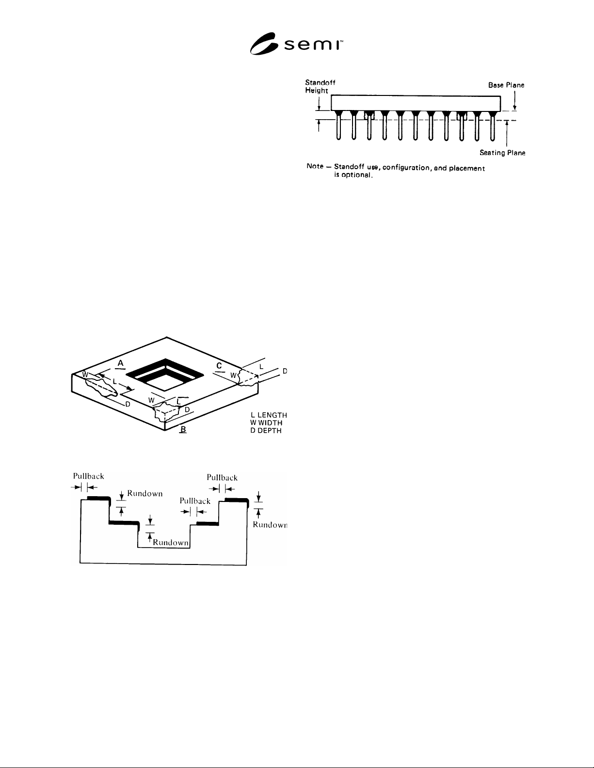
Figure 1
Chip Illustration
Figure 2
Metallization Misalignment
Figure 3
Seating Plane
NOTICE: These standards do not purport to address
safety issues, if any, associated with their use. It is the
responsibility of the user of these standards to establish
appropriate safety and health practices and determine
the applicability of regulatory limitations prior to use.
SEMI makes no warranties or representations as to the
suitability of the standards set forth herein for any
particular application. The determination of the
suitability of the standard is solely the responsibility of
the user. Users are cautioned to refer to manufacturer’s
instructions, product labels, product data sheets, and
other relevant literature respecting any materials
mentioned herein. These standards are subject to
change without notice.
The user’s attention is called to the possibility that
compliance with this standard may require use of
copyrighted material or of an invention covered by
patent rights. By publication of this standard, SEMI
takes no position respecting the validity of any patent
rights or copyrights asserted in connection with any
item mentioned in this standard. Users of this standard
are expressly advised that determination of any such
patent rights or copyrights, and the risk of infringement
of such rights, are entirely their own responsibility.
Copyright by SEMI® (Semiconductor Equipment and Materials
International), 3081 Zanker Road, San Jose, CA 95134. Reproduction o
f
the contents in whole or in part is forbidden without express written
consent of SEMI.

SEMI G34-89 © SEMI 1986, 19961
SEMI G34-89
SPECIFICATION FOR CER-PACK PACKAGE CONSTRUCTIONS,
INCLUDING LEADFRAMES, SUITABLE FOR AUTOMATED ASSEMBLY
BY END USERS
1 Preface
This specification defines the standard requirements for
Cer-Pack package construction intended for automated
assembly to printed wiring boards. Acceptance criteria
for package constructions, including leadframes, are
included.
2 Applicable Documents
1
2.1 This document specifically ref ers to:
MIL-STD-883 — Test Methods and Procedures for
Microelectronics
2.2 Related information may also be found in:
MIL-M-38510 — General Specification for
Microcircuits
3 Selected Definitions
burr — A fragment of excess material or foreign
particle adhering to the surface.
chip — Region of ceramic missing from the surface or
edge of a package which does not go completely
through the package. Chip size is given by its length,
width, and depth from a projection of the design plan-
form (see Figure 1).
crack — Cleavage or fracture that extends to the
surface of a package. It may or may not pass through
the entire thickness of the package.
critical seal area — The area bound by the shortest line
from the cavity corners to the ceramic edge (see Figure
2).
critical seal path — The nominal design distance across
the critical seal area from the die cavity to ceramic
edge.
fin — A fine, feathery-edged projection on the edge or
corner of the ceramic.
glass flow — Heated sufficiently to remove all screen
mesh marks visible at 10× magnification.
non-critical seal area — Those portions of the sealing
surface falling outside the critical area (see Figure 2).
1 Military Standards, Naval Publications and Form Center, 5801
Tabor Avenue, Philadelphia, PA 19120
overhang — Horizontal extension of glass from the
ceramic (see Figure 3).
projection — Raised portion of the surface indigenous
with the parent material.
pull back — Defines a dimension covering the linear
distance between the edge of the ceramic and the first
measurable glass interface (see Figures 3, 4, and 5).
rundown — Vertical extension of glass from the
ceramic (see Figure 3).
seal area — A dimensional outline area designated for
sealing the base and cap together to provide a hermetic
seal (see Figure 5).
void — An absence of metallization or glass from a
designated metallized or glassed area on the ceramic
surface.
4 Ordering Information
Purchase order for Cer-Pack package devices furnished
to this specification shall include the following items:
1. Drawing number and revision level
2. Type and color of ceramic
3. Type and thickness of glass
4. Type and thickness of metallization
5. Description
6. Certification by vendor
7. Method of test and measurements (see Section 9)
8. Lot acceptance procedures (see Section 8)
9. Packaging and marking (see Section 10)
10. Lead finish requirements (see Section 6.5)
5 Dimensions and Permissi ble Variations
Packaged device dimensions shall conform to JEDEC
JC-11 registered outline dimensions for Cer-Packs for
Automated Assembly.
6 Materials
6.1 Ceramic
6.1.1 Alumina content to be 90% mi nimum.