semi合集-English.pdf - 第3652页
SEMI E142-0705 © SEMI 2005 14 APPENDIX 1 WAFER MAP NOTICE : The material in this appendix is an official part of SEMI E142 and was approved by full letter ballot procedures on December 10, 2004. A1-1 This appendix shows …
SEMI E142-0705 © SEMI 2005 13
Table 20 Map Upload Parameter Dictionary
Parameter Name Description Format: Possible values
MapData The MapData to upload.
The MapData may contain one or more substrates.
Text.
Other standards that define an implementation
of this service and reference this standard will
define how the MapData is represented in
text.
Table 21 Map Upload Service Definition
Parameter Req/Ind Comment
MapData M The MapData to be uploaded. The MapData may contain one or more substrates.
SEMI E142-0705 © SEMI 2005 14
APPENDIX 1
WAFER MAP
NOTICE: The material in this appendix is an official part of SEMI E142 and was approved by full letter ballot
procedures on December 10, 2004.
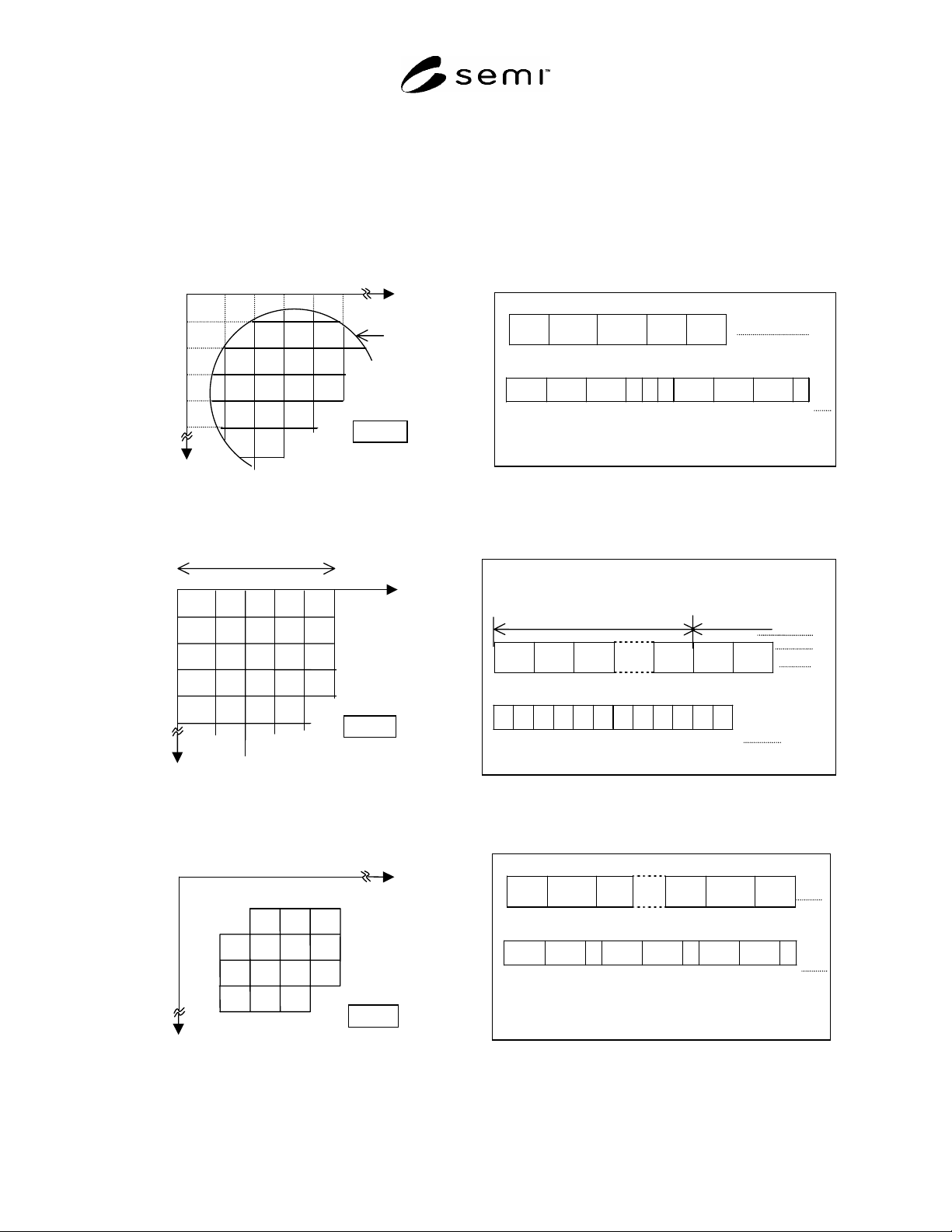
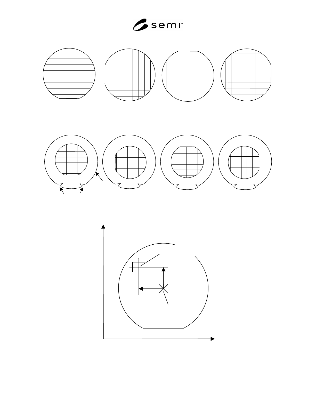
A1-1 This appendix shows how the map data items may be applied to wafers as well as some additional information
specific to this substrate type. See Figures A1-1 through A1-8.
ORIGIN
Column
Row
0
1234
0
1
2
3
4
WAFER
3
3
3
31
1
1
1
NUMBER:BIN DATA
2
2
2
2
2
2
DATA STRUCTURE
Col.
Row.
CHIP
QTY.
Bin Bin
DATA EX.
0002 0001 0003 3 1 3 0001 0002 0004 3
1
Figure A1-1a
Row/Column Format
ORIGIN
Column
Row
01 234
0
1
2
3
4
3
2
3
31
1
1
1
NUMBER:BIN DATA
2
2
2
2
2
2
DATA STRUCTURE
Bin
Bin Bin … Bin Bin Bin
DATA EX.
000000031303
1
COLUM NUMBER=5
00
00
0
00
0
0
0
Row=0
Col=0 Col=1 Col=2 Col=0
Col=1
Col=n
Row=1
Figure A1-1b
Array Format
Row
01234
0
1
2
3
4
1
1
1
1
NUMBER:BIN DATA
2
2
22
2
2
DATA STRUCTURE
Col.
Row. Bin … Col. Row. Bin
DATA EX.
0002 0001 3 0003 0001 1 0004 0001 2
Column
ORIGIN
3
3
2
3
Figure A1-1c
Coordinate Format
SEMI E142-0705 © SEMI 2005 15
0 deg. 90 deg. 180 deg. 270 deg.
Figure A1-2
Orientation of the Wafer Flat or Notch (Orientation)
FILM
FRAME
NOTCH
0 deg. 90 deg. 180 deg. 270 deg.
Figure A1-3
Orientation of the Wafer Flat or Notch on the Film Frame
+Y
+X
WAFER CENTER
REFERENCE CHIP CENTER
-x
y
Figure A1-4
Reference Device Position