semi合集-English.pdf - 第5070页
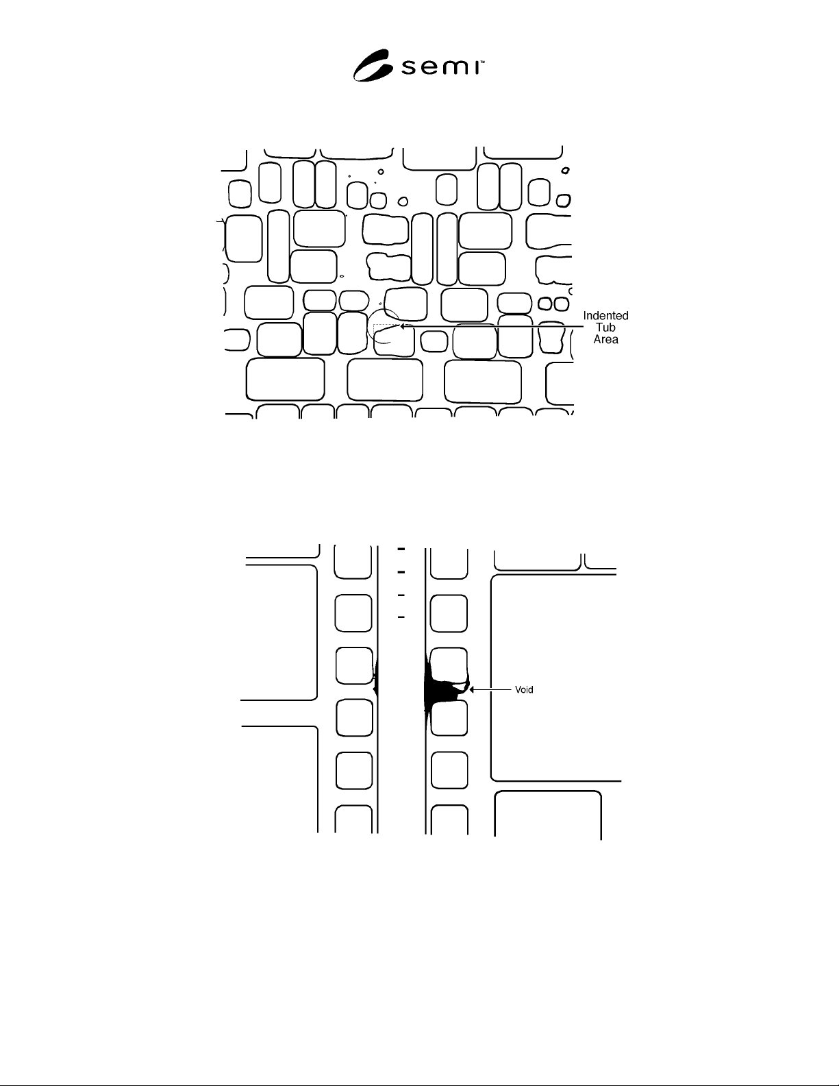
SEMI M22-0303 © SEMI 1992, 2003 5 Figure 3 Pattern Deformati on Figure 4 Void in the Polycrystalline Silicon
SEMI M22-0303 © SEMI 1992, 2003 4
packed in such a manner to avoid chipping, scratches,
and contamination, and in accordance with the best
industry practices to provide protection against damage
during shipment.
10.2 The wafers supplied under this specification shall
be identified by appropriately labeling the outside of
each box or container and each subdivision thereof in
which it may reasonably be expected that the wafers
will be stored prior to further processing. Identification
shall include supplier’s name and reference no., date,
quantity, DI wafer diameter, DI wafer thickness, and
customer code no. The reference number assigned by
the supplier shall provide ready access to information
concerning the fabrication history of the particular
wafers in that lot. Such information shall be retained on
file at the manufacturer’s facility for at least one year
after the particular lot has been shipped.
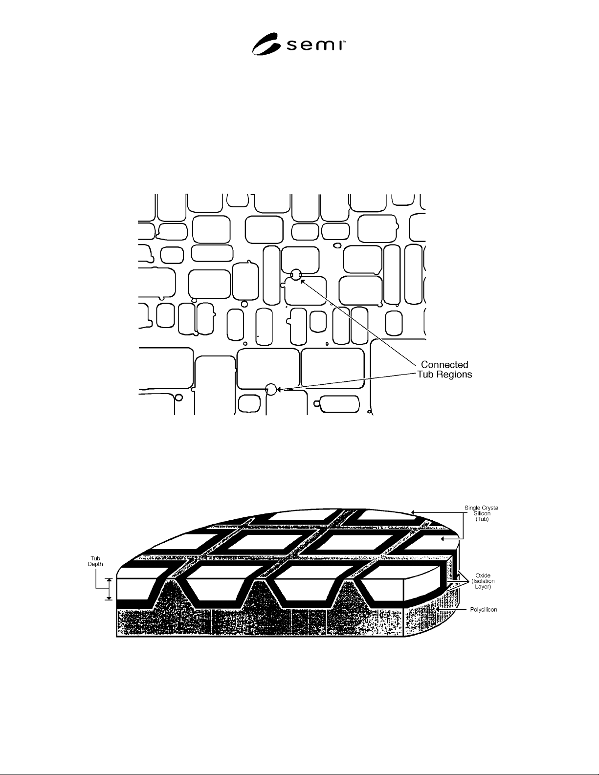
Figure 1
Connected Tubs
Figure 2
Cross-Section of DI Wafer
SEMI M22-0303 © SEMI 1992, 2003 5
Figure 3
Pattern Deformation
Figure 4
Void in the Polycrystalline Silicon
SEMI M22-0303 © SEMI 1992, 2003 6
NOTICE: SEMI makes no warranties or representations as to the suitability of the standard set forth herein for any
particular application. The determination of the suitability of the standard is solely the responsibility of the user.
Users are cautioned to refer to manufacturer’s instructions, product labels, product data sheets, and other relevant
literature respecting any materials or equipment mentioned herein. These standards are subject to change without
notice.
By publication of this standard, SEMI takes no position respecting the validity of any patent rights or copyrights
asserted in connection with any item mentioned in this standard. Users of this standard are expressly advised that
determination of any such patent rights or copyrights, and the risk of infringement of such rights, are entirely their
own responsibility.
Copyright by SEMI® (Semiconductor Equipment and Materials
International), 3081 Zanker Road, San Jose, CA 95134. Reproduction o
f
the contents in whole or in part is forbidden without express written
consent of SEMI.