semi合集-English.pdf - 第2587页
SEMI E90-0705 © SEMI 1999, 2005 27 RELATED INFORMATION 1 NOTICE : This related information is not an official part of SEMI E90. This related information was ap proved for publication by full letter ballot proced ures on …
SEMI E90-0705 © SEMI 1999, 2005 26
15 Requirements for Compliance
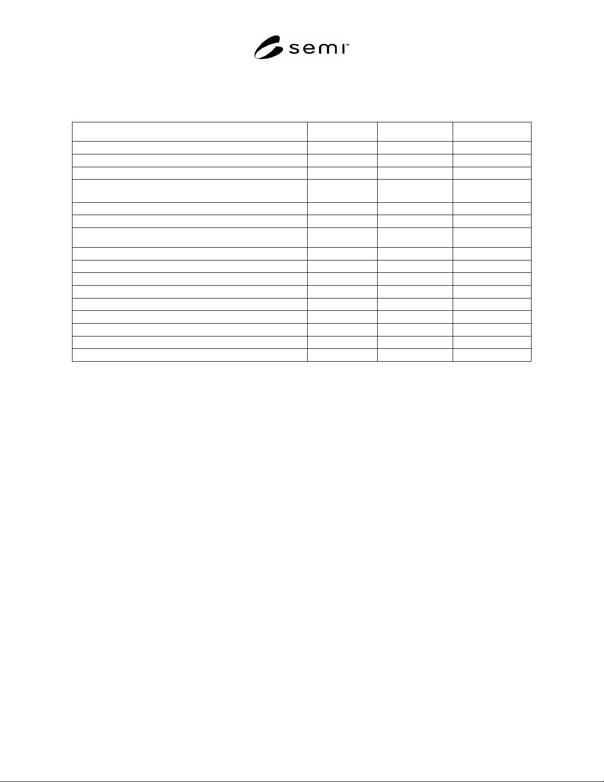
15.1 Table 19 provides a checklist for Substrate Tracking (STS) compliance.
Table 19 STS Compliance Statement
Fundamental STS Requirements STS Section Implemented STS Compliant
Substrate Tracking 8 (except 8.4) Yes No Yes No
Substrate Object and State Model 9 Yes No Yes No
Substrate Location Object and State Model 10 Yes No Yes No
Service Message Implementation (except host-initiated Register
(Create) Substrate and Remove Substrate)
12 Yes No Yes No
Variable Data 13 Yes No Yes No
Events 8.4 Yes No Yes No
Additional STS Capabilities STS Section Implemented STS Compliant
Host-Initiated Register (Create Substrate) 12.1.1 Yes No Yes No
Host-Initiated Remove Substrate Yes No Yes No
Batch Location Object and State Model 11 Yes No Yes No
UpdateSubstrateObject service 12 Yes No Yes No
Substrate Reading Status 9.3 Yes No Yes No
"SubstIDStatus" substrate object attribute 9.5 Yes No Yes No
ProceedWithSubstrate service 12.2 Yes No Yes No
CancelSubstrate service 12.2 Yes No Yes No
Additional Events 14 Yes No Yes No
SEMI E90-0705 © SEMI 1999, 2005 27
RELATED INFORMATION 1
NOTICE: This related information is not an official part of SEMI E90. This related information was approved for
publication by full letter ballot procedures on January 14, 2000.
R1-1 Substrate State Model Implementation
R1-1.1 The Substrate Object State Model defined in ¶9.1 is a generic representation of the substrate object state
model that includes standard transitions for various equipment types.
R1-1.2 Some equipment may not be able to implement all of the transitions defined in this model. For example, the
transition from AT WORK to AT SOURCE (Transition Number 3) represents the case where the substrate returns to
the original (source) location, typically for further processing. If the equipment is unable to implement this return,
then the transition would never occur, and it should be omitted from the implemented state model.
R1-1.3 The state model shall be implemented based on the definition of the state model; however, substates and
transitions that cannot occur for a particular equipment design may be omitted where the model allows.
R1-2 Example of Substrate Object State Model for Simple Equipment
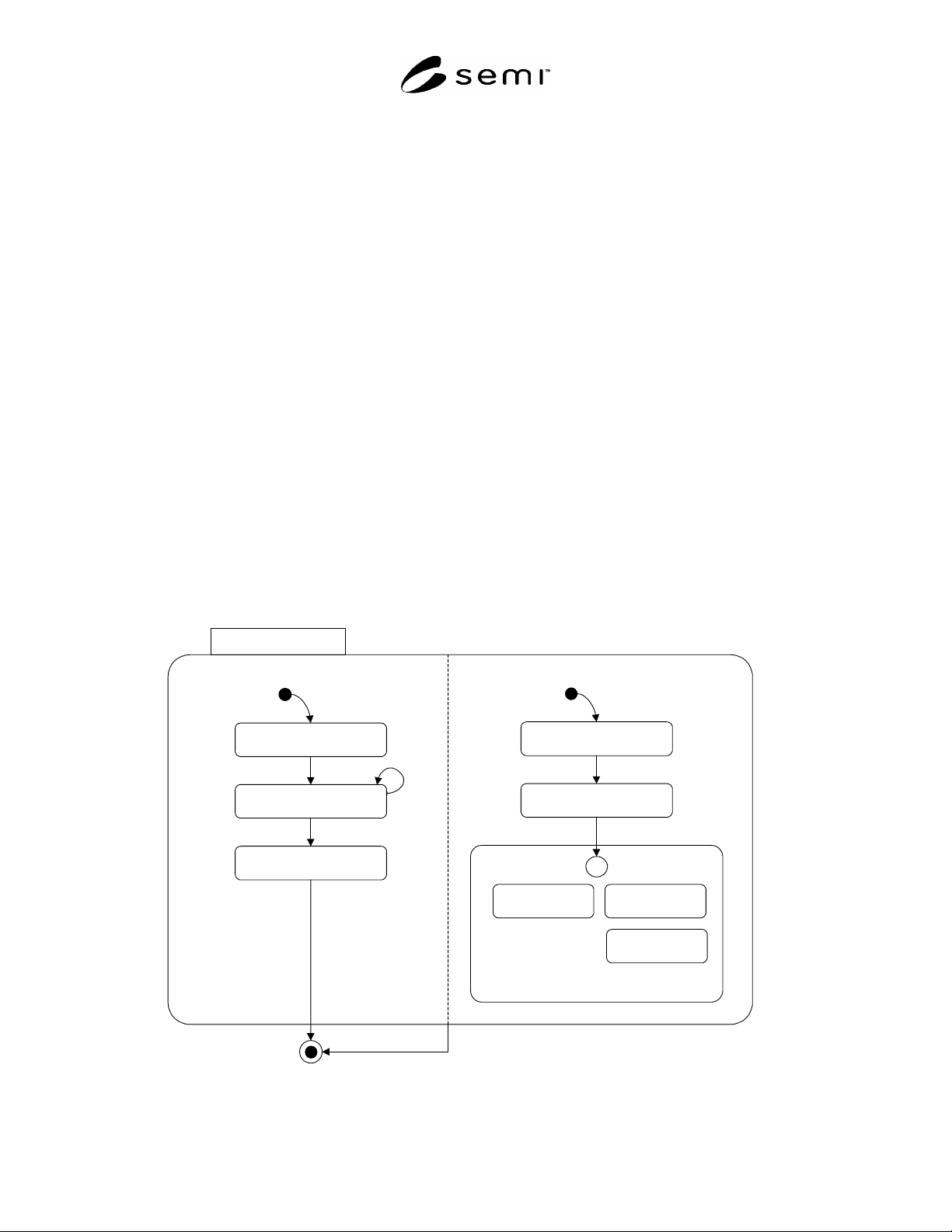
R1-2.1 This section shows an example of Substrate Object State Model for simple equipment. (See Figure R1-1.)
R1-2.2 The equipment transports the substrate only in a forward direction, so that the Substrate Transport Substate
takes straight forward transitions from AT SOURCE to AT WORK and then to AT DESTINATION. For example,
the wirebonder removes leadframes from a magazine and carries them on a transport mechanism but is unable to
return them to the magazine.
R1-2.3 Also, the equipment processes the substrate only in forward steps so that the Substrate Processing Substate
takes straight forward transitions from NEED PROCESSING to IN PROCESS and then to PROCESSING
COMPLETE. The REJECTED state is not applied to this equipment.
SUBSTRATE
IN PROCESS
NEEDS PROCESSING
PROCESSED
C
ABORTED
STOPPED
AT SOURCE
AT WORK
AT DESTINATION
PROCESSING COMPLETE
1
9
7
5
2
10
12
11
SUBSTRATE PROCESSING
SUBSTRATE TRANSPORT
4
Figure R1-1
Substrate State Model for Simple Equipment

SEMI E90-0705 © SEMI 1999, 2005 28
NOTICE: SEMI makes no warranties or representations as to the suitability of the standards set forth herein for any
particular application. The determination of the suitability of the standard is solely the responsibility of the user.
Users are cautioned to refer to manufacturer's instructions, product labels, product data sheets, and other relevant
literature, respecting any materials or equipment mentioned herein. These standards are subject to change without
notice.
By publication of this standard, Semiconductor Equipment and Materials International (SEMI) takes no position
respecting the validity of any patent rights or copyrights asserted in connection with any items mentioned in this
standard. Users of this standard are expressly advised that determination of any such patent rights or copyrights, and
the risk of infringement of such rights are entirely their own responsibility.
Copyright by SEMI® (Semiconductor Equipment and Materials
International), 3081 Zanker Road, San Jose, CA 95134. Reproduction of
the contents in whole or in part is forbidden without express written
consent of SEMI.