semi合集-English.pdf - 第4514页
SEMI D24-0200 © SEMI 2000 4 (Pat tern Surfac e) Length (L) Width (W) Short Reference Edge (S RE) Orientation Corner Long Reference Edge (LRE) Figure 1 Reference Items (Pat tern Surf ace) Shor t Re ference Edge (SR E) 1 O…
SEMI D24-0200 © SEMI 20003
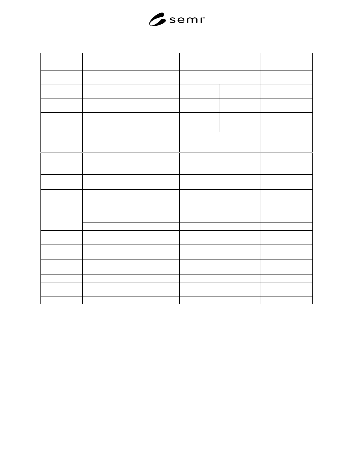
Table 1 Specification for Gen III and Larger Active-Matrix LCD Substrates
Reference
Information
Range A Range B Reference Documents
Edge Length
Ranges
550 to 650 mm × 650 to 830 mm 750 to1000 mm × 900 to 1100 mm
Edge Length
Dimensions
600 × 720 mm, 650 × 830 mm,
550 × 650 mm
800 × 950 mm 900 × 1100 mm
Edge Length
Tolerance
1
± 0.40 mm ± 0.40 mm ± 0.50 mm SEMI D5 – Std. Sizes
for FPD Substrates
Squareness
1
± 0.83 mm W = ± 0.80 mm
L = ± 0.95 mm
± 1.0 mm SEMI D4 –
Referencing of FPD
Substrates
Edge Condition
9
Rounded
9
Bevel width = 0.1 mm – 0.6 mm, —
extension onto top/bottom surfaces
Rounded
9
Bevel width = 0.1 mm – 0.6 mm
Orientation
Corner
2
1 Corner, Symmetric
C1x = 4.0 ± 1.0 mm
C1y = 4.0 ± 1.0 mm
1 Corner, Asymmetric
C1x = 5.0 ± 1.5 mm
C1y = 2.0 ± 1.5 mm
1 Corner, Asymmetric
C1x = 5.0 ± 1.5 mm
C1y = 2.0 ± 1.5 mm
Corner Cut 3 corners
C2x & C2y = 1.5 ± 1.0 mm
3 corners
C2x & C2y = 1.5 ± 1.0 mm
SEMI D12 – Edge
Condition
Quality Area
3
Edge Exclusion
≤ 10 mm ≤ 20 mm
11
SEMI D3 – Quality
Area for FPD
Substrates
0.7 mm ± 0.07 mm 0.7 mm ± 0.07 mm
SEMI D5 – Std. Sizes
for FPD Substrates
Thickness
1.1 mm ± 0.10 mm 1.1 mm ± 0.10 mm
Total Thickness
Variation
4
60 µm 100 µm
Local Thickness
Variation
5
≤ 20 µm for ≤ 130 mm ≤ 20 µm for ≤ 130 mm
Waviness
6
[W
fpd
]
≤ 0.1 µm, with
λ
C
= 0.8 mm, λ
L
= 8 mm L
S
= 20 mm
≤ 0.1 µm, with
λ
C
= 0.8 mm, λ
L
= 8 mm L
S
= 20 mm
SEMI D15 – Surface
Waviness Measurement
Warp
7
≤ 0.60 mm ≤ 1.0 mm
Roughness, R
a
≤ 20 nm ≤ 20 nm SEMI D7 – Roughness
Measurement
Straightness
8
± 0.4 mm ± 0.4 mm
NOTES:
1 For dimensional tolerance and squareness the long edge typically has the maximum tolerance. See Figures 1 and 2.
2 An asymmetric orientation corner is specified for purposes of mechanical orientation and operator’s visual confirmation of orientation within a
cassette. Optical means of identifying orientation is under investigation. See Figure 5.
3 Quality Area is that area in which the specified criteria apply.
4 Total thickness variation is the peak to valley (TIR) of the entire substrate front surface relative to a reference plane when the substrate back
surface is constrained against a vacuum chuck. This scale is typically important for some film deposition and lithography processes. See Figure
6.
5 Local thickness variation
is the absolute value of the maximum deviation of the substrate from a plane constructed in any 100–130 mm square
area, within the Quality Area, when the substrate back surface is constrained against a vacuum chuck. This scale is typically important for
lithographic stepper processes.
6 Waviness is the rms (root mean square) surface profile, within the quality area, over 0.8–8 mm spatial wavelengths.
7 See Figure 3.
8 See Figure 2.
9 See Figure 4.
10 This table applies to the indicated edge length ranges and thicknesses.
11 Example: For an 800 × 950 mm substrate, the effective process area, which excludes portions not processable for physical reasons, would be ≥
760 × ≥ 910 mm.
SEMI D24-0200 © SEMI 2000 4
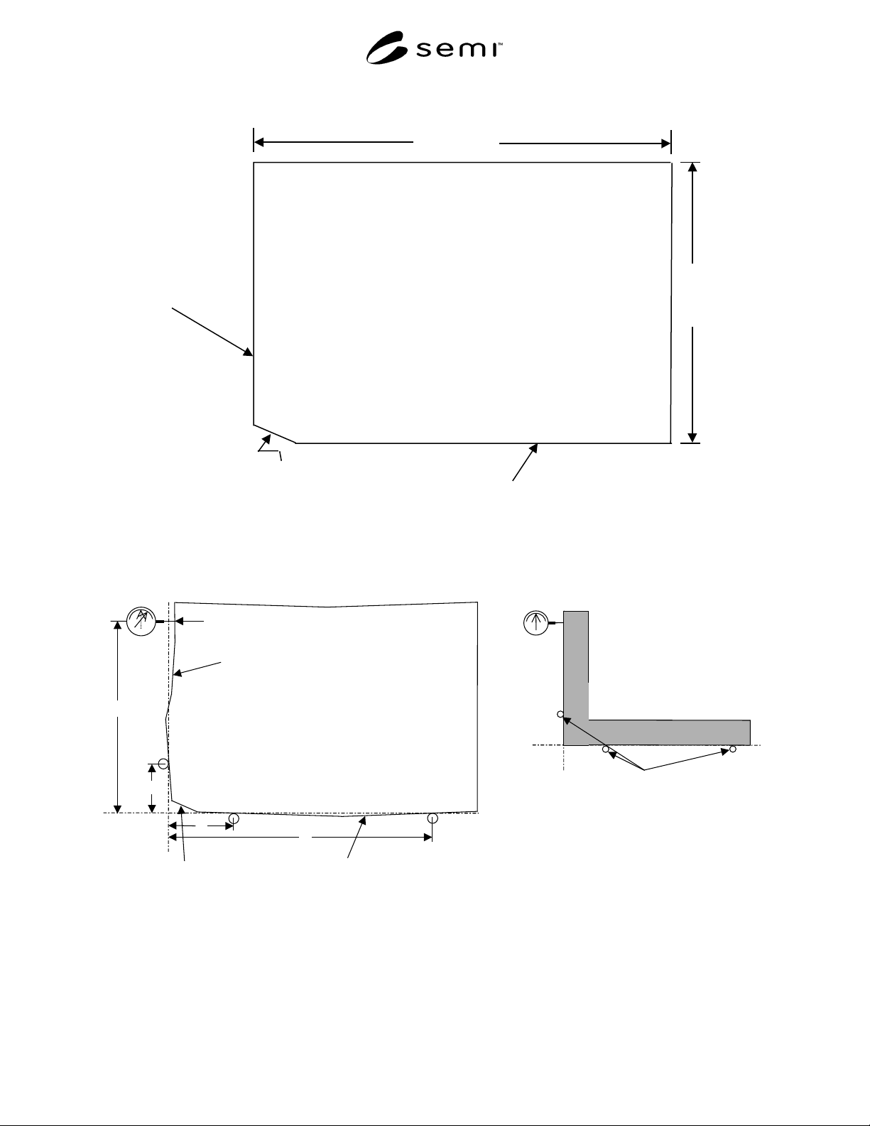
(Pattern Surface)
Length (L)
Width (W)
Short Reference
Edge (SRE)
Orientation Corner
Long Reference Edge (LRE)
Figure 1
Reference Items
(Pattern Surface)
Short Reference Edge (SRE)
1 Orientation Corner
Long Reference Edge (LRE)
Dial
Gauge
Pr
a
b
c
d
Calibration using Square
Gauge
Dial
Gauge
Zero
Support pins
NOTE: a, b, c, and d are defined between supplier and customer.
Figure 2
Squareness
SEMI D24-0200 © SEMI 20005
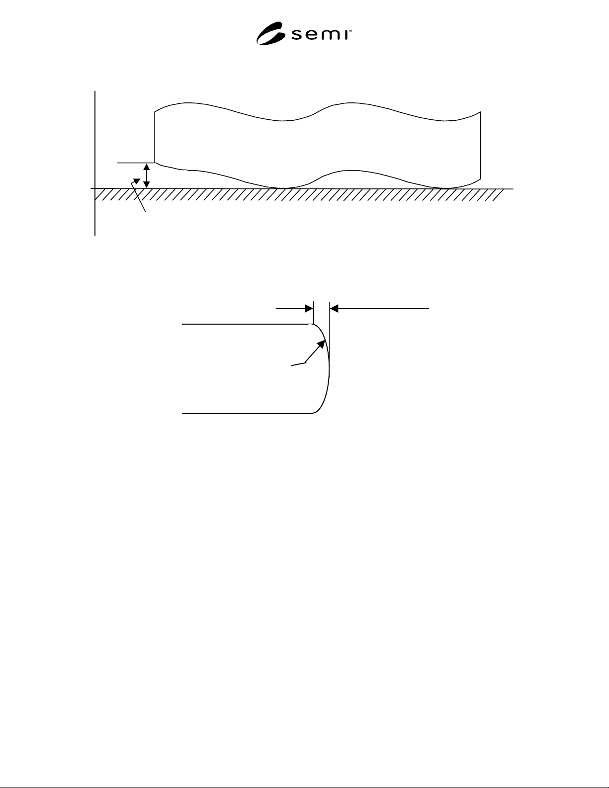
Warp
Detected along edge by feeler gauge
(Back Surface Unconstrained)
X
Z
0
Figure 3
Warp
Rounded bevel
0.1 - 0.6 mm
Figure 4
Edge Condition