semi合集-English.pdf - 第7453页
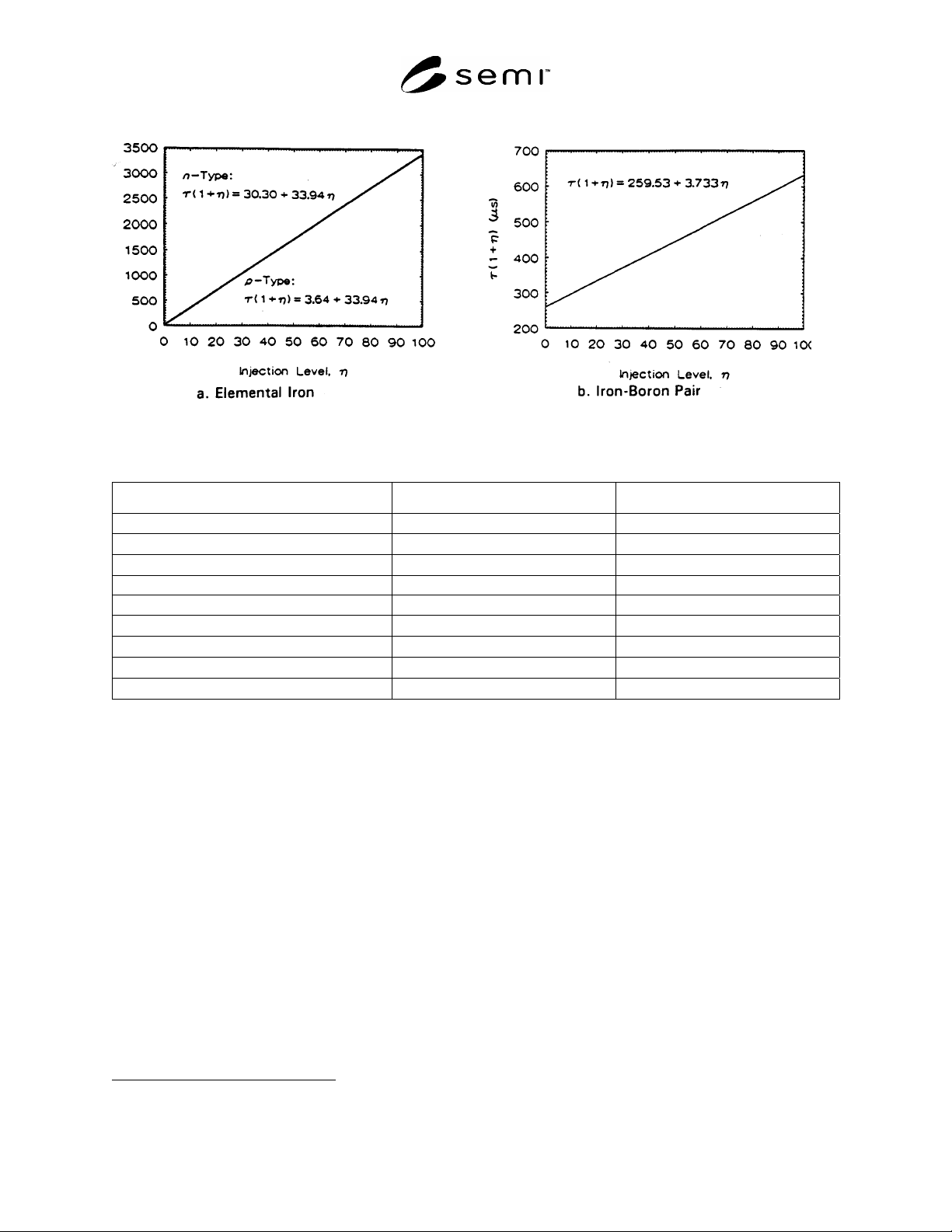
SEMI MF1535-1104 © SEMI 2004 11 Figure R1-1 Derivation of 0 and from Plots of Recombination Lifetime versus Injection Level Table R1-1 Parameters Us ed for Calculation of Recombination Life time versus Injection Le…

SEMI MF1535-1104 © SEMI 2004 10
RELATED INFORMATION 1
INJECTION LEVEL CONSIDERATIONS
NOTICE: This related information is not an official part of SEMI MF1535. It was derived from
information developed during the original preparation of the standard in ASTM Committee F-1 in 1994.
This related information was approved for publication by full letter ballot procedures.
R1-1 The carrier recombination lifetime is frequently
associated with the minority carrier lifetime. This
association is correct only if the lifetime is determined
for low injection level when
(the ratio of density of
excess photogenerated carriers to the equilibrium
density of majority carriers) is much less than 1, and
then only if certain other conditions are also met (see
Related Information 2 and Related Information 3).
Nevertheless, the low-injection (small-signal) value of
the carrier recombination lifetime is independent of the
exact value of
provided that
<< 1. However, in this
test method, it is often neither possible nor convenient
to make measurements in the low-injection regime.
When this is the case, the measured recombination
lifetime is a function of the injection level.
R1-2 The basic model for carrier recombination
through defect centers in semiconductors was
developed independently by Hall
14
and by Shockley
and Read.
15
This model has been thoroughly discussed
by Blakemore.
16
In the Shockley-Read-Hall (S-R-H)
model, it is assumed (1) that the doping level of the
semiconductor is not so high that the semiconductor
becomes degenerate, and (2) that the density of defect
centers is small compared with the majority carrier
density.
NOTE 1: The reader should refer to Blakemore’s text for a
more complete treatment than is presented here, including the
derivation of the S-R-H expression (Equation R1-1) for
carrier lifetime and discussion of the effect of Fermi energy
on the small-signal recombination lifetime. In addition,
Blakemore goes on to discuss other complexities that result
when the density of defect centers is not small compared with
the majority carrier density,
17
and when carrier trapping
occurs.
18
R1-3 Both the assumptions underlying the S-R-H
model are generally appropriate for the specimens to be
measured by this test method. With these assumptions,
the density of excess electrons (n
e
) is equal to the
density of excess holes (p
e
), and the electron (
n
) and
hole (
p
) lifetimes for recombination through a defect
14 Hall, R. N., “Electron-Hole Recombination in Germanium,”
Phys. Rev. 87, 387 (1952).
15 Shockley, W., and Read, W. T., “Statistics of the Recombination
of Holes and Electrons,” Phys. Rev. 87, 835–842 (1952).
16 Blakemore, J. S., op. cit., Section 8.3.
17 Blakemore, J. S., op. cit., Sections 8.4 and 8.5.
18 Blakemore, J. S., op. cit., Section 8.2.
center located at an energy
T
within the forbidden
energy gap are equal. This carrier recombination
lifetime, , in s, is given as follows:
)(
)()(
00
100100
e
epen
pn
npn
nnnnpp
(R1-1)
where:
n0
= time constant for ca
p
ture of an electron in an
empty center, in s,
p0
= time constant for capture of a hole in a filled
center, in s,
n
0
= equilibrium density of electrons in a
nondegenerate semiconductor, in electrons/cm
3
,
p
0
= equilibrium density of holes in a nondegenerate
semiconductor, in holes/cm
3
,
n
1
= density of electrons in a nondegenerate
semiconductor when the Fermi energy,
F
, =
T
, in
electrons/cm
3
, and
p
1
= density of holes in a nondegenerate semiconductor
when the Fermi energy,
F
, =
T
, in holes/cm
3
.
R1-4 In the low-injection limit, n
e
can be neglected
and Equation R1-1 reduces to the small-signal
recombination lifetime,
0
.
)(
)(
)(
)(
00
10
0
00
10
00
pn
nn
np
pp
pn
(R1-2)
On the other hand, in the high-injection limit, n
e
is the
dominant term and the recombination lifetime becomes:
00 pn
(R1-3)
At intermediate injection levels the recombination
lifetime can be expressed as a combination of
0
and
:
1
)(
0
00
000
e
e
npn
npn
(R1-4)
Therefore, a straight line is obtained when the quantity
(1+
) is plotted against
. The zero intercept of this
line is
0
and its slope is
. The linearity of this
function provides a test for the validity of the S-R-H
model and also for the presence of multiple defect
centers in the test specimen.
SEMI MF1535-1104 © SEMI 2004 11
Figure R1-1
Derivation of
0
and
from Plots of Recombination Lifetime versus Injection Level
Table R1-1 Parameters Used for Calculation of Recombination Lifetime versus Injection Level
Parameter Elemental Iron (Fe) Iron-Boron (Fe-B)
Temperature, K 300 300
Boron density (p
0
), cm
3
1 × 10
15
1 × 10
15
n
0
, cm
3
1.16 × 10
5
1.16 × 10
5
Iron density, atoms/cm
3
5 × 10
11
5 × 10
11
Defect energy, eV (above valence band edge) 0.400 0.100
n0
, s
3.64 0.400
p0
, s
30.3 3.33
n
1
, cm
3
1.96 × 10
7
179
p
1
, cm
3
5.91 × 10
12
6.48 × 10
17
R1-5 This linearity is illustrated in Figure R1-1 for
recombination through the elemental iron defect center
in both n- and p-type silicon and through iron-boron
pairs in p-type silicon. The parameters for the
calculations are listed in Table R1-1; in each case it is
assumed that all of the iron is in the defect state listed.
Note that for elemental iron in p-type silicon,
0
=
n0
, for
the iron-boron pair,
0
>>
n0
; and for elemental iron in n-
type silicon,
0
=
p0
.
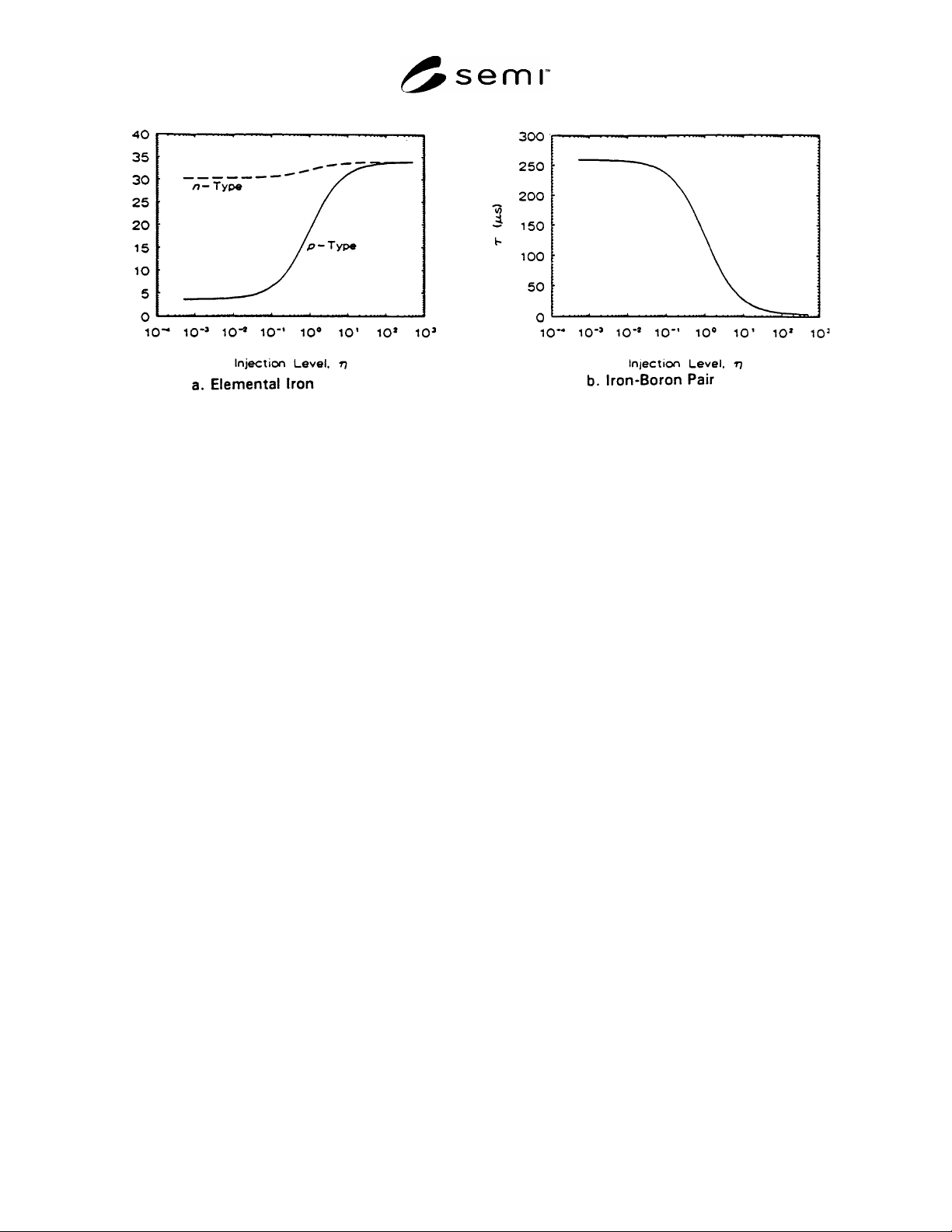
R1-6 Injection level spectroscopy, which has been
proposed
3
as a method for identifying impurity levels,
relies on the relationship between
0
and
as a
function of the density of the impurity center for
specific doping conditions. This method is particularly
useful for studying iron in p -type silicon because of the
facts that (1) it is possible to treat the sample to ensure
that essentially all of the iron is in either the elemental
or paired state,
19
and (2) the injection level dependence
19 Zoth, G., and Bergholz, W., “A Fast, Preparation-Free Method to
Detect Iron in Silicon,” J. Appl. Phys. 67, 6764–6771 (1990).
is markedly different for the two species (see Fig. R1-
2).
R1-7 However, it should be noted that if several
contaminants are present at the same time at similar
concentrations, the measured ratio of
0
to
may
represent some average of the values for the various
contaminants because this technique is not impurity
specific as is deep-level transient spectroscopy or other
spectroscopic techniques involving filling and emptying
of defect centers in the space-charge layer.
SEMI MF1535-1104 © SEMI 2004 12
Figure R1-2
Recombination Lifetime as a Function of Injection Level