semi合集-English.pdf - 第5885页
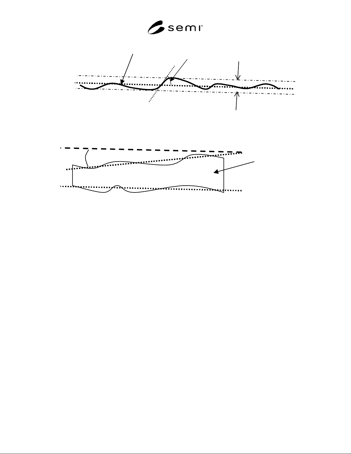
SEMI P37-1102 © SEMI 2001, 2002 7 P 1 Mask substra te surface Flatnes s error Local slope angle Figure 4 Definition of Flatne ss Error and L ocal Slope Angle P1 is the plane th at mi nimizes maximum devia tion of the sur…
SEMI P37-1102 © SEMI 2001, 2002 6
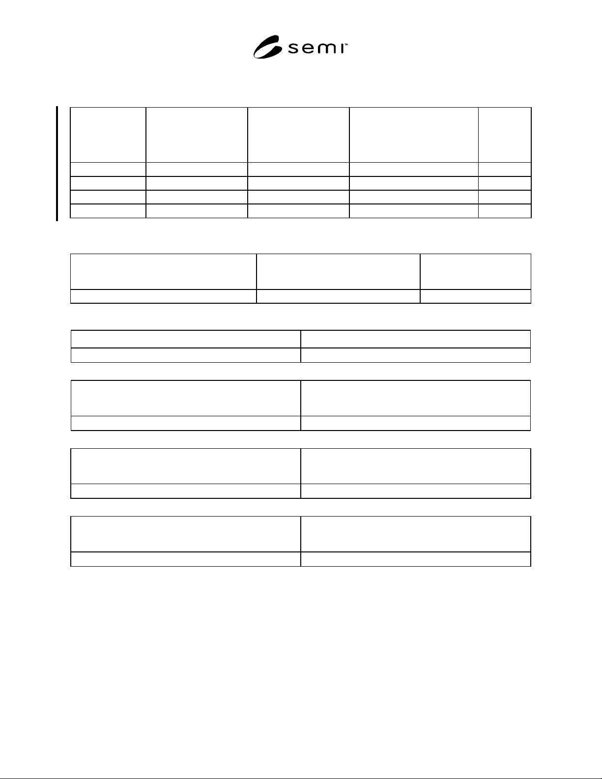
Table 4 Flatness, Wedge and Surface Roughness
FLATNESS ERROR IN FLATNESS QUALITY AREA
Class Frontside Flatness, within
Flatness Quality Area
Backside Flatness, within
Flatness Quality Area
Low Order Thickness Variation
(LOTV), within Flatness Quality
Area (See Note 2.)
λ
spatial
> (edge length)
Units
A 100 peak-to-valley 100 peak-to-valley 100 nm
B 75 peak-to-valley 75 peak-to-valley 75 nm
C 50 peak-to-valley 50 peak-to-valley 50 nm
D 30 peak-to-valley 30 peak-to-valley 30 nm
NOTE 1: λ
spatial
is the spatial period of the flatness error.
NOTE 2: Evaluated after removing wedge angle.
FLATNESS OVER ENTIRE SURFACE
Frontside Flatness
λ
spatial
≤
(edge length)
Backside Flatness
λ
spatial
≤
(edge length)
Units
1000 peak-to-valley 1000 peak-to-valley nm
NOTE 1: λ
spatial
is the spatial period of the flatness error.
WEDGE
Wedge angle Units
≤ 100
microradians
LOCAL SLOPE OF FRONT SURFACE
Local slope angle
400 nm
≤
λ
spatial
≤
100 mm
Units
≤ 1.0
milliradians
FRONT SIDE SURFACE ROUGHNESS
Surface Roughness in Quality Area (Figure 6),
λ
spatial
≤
10
µ
m
Units
≤ 0.15 rms
nm
BACK SIDE SURFACE ROUGHNESS
Surface Roughness over entire back surface,
50 nm
≤
λ
spatial
≤
10
µ
m
Units
≤ 0.5 rms
nm
NOTE 1: rms is root mean square error. λ
spatial
is the
spatial wavelength of the roughness.
SEMI P37-1102 © SEMI 2001, 2002 7
P
1
Mask substrate surface
Flatness error
Local slope
angle
Figure 4
Definition of Flatness Error and Local Slope Angle
P1 is the plane that minimizes maximum deviation of the surface.
α
Mask substrate
P
1
´
P
2
P
1
P
1
´ || P
1
Figure 5
Definition of Wedge Angle,
α
P
1
and P
2
are the planes that minimize the maximum deviation of the front and back surfaces, respectively.
SEMI P37-1102 © SEMI 2001, 2002 8
L
D
W
Defect
quality
area
L
Figure 6
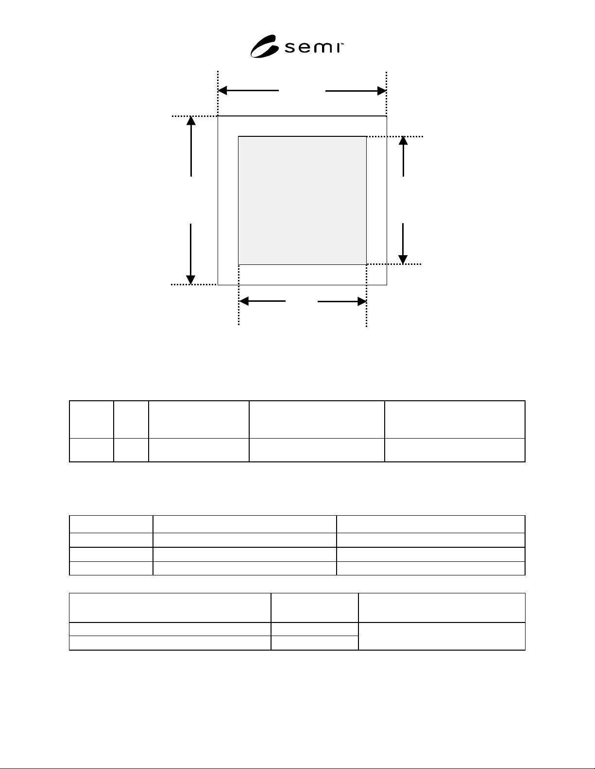
Definition of defect quality area on front side
Table 5 Substrate Defect Limits per Plate
FRONTSIDE SURFACE DEFECTS IN THE DEFECT QUALITY AREA
Frontside
Residue
Total Scratch and Sleek
Defects > 1 nm in depth
(See Note 1.)
Total Localized Light Scatterers > 50
nm PSL equivalent size (per cm
2
)
(See Note 2.)
Total Localized Light Scatterers < 50
nm PSL equivalent size (per cm
2
)
(See Note 2.)
NZTE None 0 0 To be agreed upon between user and
supplier
NOTE 1: The maximum size for scratches and sleeks will be agreed upon between user and supplier.
NOTE 2: Localized light scatterers are any isolated features, such as particles or pits, on or in the substrate surface, resulting in increased light
scattering intensity relative to that of the surrounding substrate surface. PSL equivalent size means the detected defect appears to be the same
size as a polystyrene latex sphere examined under the same inspection conditions.
FRONTSIDE DEFECTS OUTSIDE THE DEFECT QUALITY AREA
Edge Chips Defect Limit Total Number
Radial Depth
≥ 0.76 mm
None
Peripheral Cord
≥ 0.76 mm
None
Other Shall be negotiated between vendor and supplier Shall be negotiated between vendor and supplier
BACKSIDE DEFECTS IN FLATNESS QUALITY AREA
Localized Light Scatterer Size (PSL equivalent)
(See Note 2.)
Total Total Number of Backside Scratches
(See Note 1.)
> 1.0 µm
0
≤ 1.0 µm
no limit
0
NOTE 1: The maximum size for scratches and sleeks will be agreed upon between user and supplier.
NOTE 2: Localized light scatterers are any isolated features, such as particles or pits, on or in the substrate surface, resulting in increased light
scattering intensity relative to that of the surrounding substrate surface. PSL equivalent size means the detected defect appears to be the same
size as a polystyrene latex sphere examined under the same inspection conditions.