semi合集-English.pdf - 第7553页
SEMI MF1810-0304 © SEMI 2003, 2004 6 Figure R1-1 95% Confidence Interval B ox and Wh isker Plot for 16 Laboratories NOTICE: SEMI makes no warranties or represen tations as to the suitability o f the standards set forth h…
SEMI MF1810-0304 © SEMI 2003, 2004 5
RELATED INFORMATION 1
SUMMARY OF MULTI LABORATORY ROUND ROBIN TEST
NOTICE: This related information is not an official part of SEMI MF1810. It was developed as part of
the development of the document. This related information was approved for publication by full letter
ballot on December 4, 2004.
R1-1 The multilaboratory round robin test was done
over a period of 12 months and included 16
laboratories. The test required each laboratory to
complete 11 diameter scan measurements of seven
wafers. A “diameter scan” area is equal to the area
defined by a microscope field of view and a length
equal to the wafer diameter less the edge exclusion.
Only one defect classification, OISF, was included in
the count and described with pictures. The sequence
and path of the measurement scans were defined so that
the comparison of the individual measurements would
be possible among data sets. Within the ability of each
laboratory to align the sample on the microscope stage,
the starting point and scan path was held constant.
R1-2 The complete repeatability and reproducibility
study results are listed in Table R1-1 for the four scan
method for the parameter, deviation from target, in
units of defects/cm
2
. The average range was 2.107 and
the range of x-bars was 12.130.
Table R1-1 Repeatability and Reproducibility for 16
Laboratories, Seven Samples, and Two Trials
Estimated
Sigma
Estimated
Variance
Percent of
Total
Repeatability 1.863 3.472 23.92
Reproducibility 3.323 11.045 76.08
Repeatability and
Reproducibility
3.810 14.517 100.00
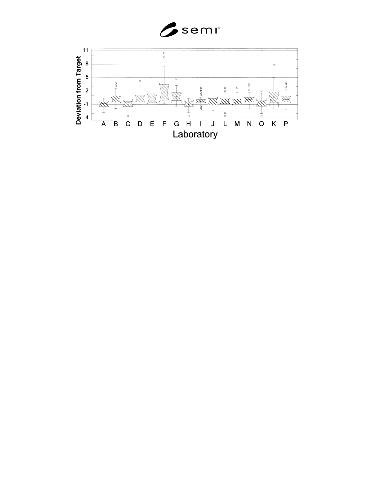
R1-3 A multiple range test by the 95% least squares
deviation (LSD) method for the deviation from target
by laboratory was done. Results are shown in Table
R1-2. Differences among laboratories are also evident
in the 95% confidence interval box and whisker plot
provided in Figure R1-1, which shows the deviation
from target for each laboratory. This plot is based on
four diameter scans per test.
R1-4 Results from Laboratory F were significantly
different from all other laboratories, but were included
in the reported Precision and Bias Section because no
evidence pointed to a procedural mistake. The
alternative repeatability and reproducibility study
results are listed in Table R1-3 for the four scan method
for the parameter, deviation from target, in units of
defects/cm
2
. In this case, the average range was 1.930
and the range of x-bars was 7.018.
Table R1-2 Multiple Range Test for 16 Laboratories
Laboratory Count
Least
Squares
Mean
Homogeneous
Groups
H 77 –0.948022 X
C 77 –0.948002 X
A 77 –0.868478 XX
O 77 –0.635124 XXX
M 77 –0.469934 XX
J 77 –0.437819 X
I 77 –0.28686 XX
L 77 –0.261265 XX
N 77 0.064319 XX
P 77 0.176689 XX
B 77 0.403837 XX
E 77 0.406758 XX
K 77 0.425747 XXX
D 77 0.549704 XX
G 77 0.816097 X
F 77 2.01237 X
Table R1-3 Repeatability and Reproducibility for 16
Laboratories, Seven Samples, and Two Trials
Estimated
Sigma
Estimated
Variance
Percent of
Total
Repeatability 1.707 2.912 44.08
Reproducibility 1.922 3.695 55.92
Repeatability and
Reproducibility
2.570 6.607 100.00
SEMI MF1810-0304 © SEMI 2003, 2004 6
Figure R1-1
95% Confidence Interval Box and Whisker Plot for 16 Laboratories
NOTICE: SEMI makes no warranties or representations as to the suitability of the standards set forth herein for any
particular application. The determination of the suitability of the standard is solely the responsibility of the user.
Users are cautioned to refer to manufacturer' s instructions, product labels, product data sheets, and other relevant
literature, respecting any materials or equipment mentioned herein. These standards are subject to change without
notice.
By publication of this standard, Semiconductor Equipment and Materials International (SEMI) takes no position
respecting the validity of any patent rights or copyrights asserted in connection with any items mentioned in this
standard. Users of this standard are expressly advised that determination of any such patent rights or copyrights, and
the risk of infringement of such rights are entirely their own responsibility.
Copyright by SEMI® (Semiconductor Equipment and Materials
International), 3081 Zanker Road, San Jose, CA 95134. Reproduction o
f
the contents in whole or in part is forbidden without express written
consent of SEMI.

SEMI MF1811-0704 © SEMI 2003, 2004 1
SEMI MF1811-0704
GUIDE FOR ESTIMATING THE POWER SPECTRAL DENSITY
FUNCTION AND RELATED FINISH PARAMETERS FROM SURFACE
PROFILE DATA
This guide was technically approved by the Global Silicon Wafer Committee and is the direct responsibility
of the North American Silicon Wafer Committee. Current edition approved for publication by the North
American Regional Standards Committee on March 14, 2004. Initially available at
www.semi.org May
2004; to be published July 2004. Original edition published by ASTM International as ASTM F 1811-97.
Last previous edition SEMI MF1811-97(2002).
1 Purpose
1.1 There is some confusion in the roughness-
measurement community concerning the use of
estimators and the calculation of power spectral
densities (PSDs) from discrete data sets. Use of this
guide can eliminate these differences and result in the
use of consistent units for the PSD and related
parameters. It also provides a uniform reporting
procedure for digital roughness data that can facilitate
communication between different workers and different
laboratories.
2 Scope
2.1 This guide defines the methodology for calculating
a set of commonly used statistical parameters and
functions of surface roughness from a set of measured
surface profile data. Its purposes are to provide
fundamental procedures and notation for processing and
presenting data, to alert the reader to related issues that
may arise in user-specific applications, and to provide
literature references where further details can be found.
2.2 This guide is limited to the analysis of one-
dimensional or profile data taken at uniform intervals
along straight lines across the surface under test,
although reference is made to the more general case of
two-dimensional measurements made over a
rectangular array of data points.
2.3 The data analysis procedures described in this
guide are generic and are not limited to specific
surfaces, surface-generation techniques, degrees of
roughness, or measuring techniques. Examples of
measuring techniques that can be used to generate
profile data for analysis are mechanical profiling
instruments using a rigid contacting probe, optical
profiling instruments that sample over a line or an array
over an area of the surface, optical interferometry, and
scanning-microscopy techniques such as atomic-force
microscopy. The distinctions between different
measuring techniques enter this guide through various
parameters and functions that are defined in Sections 4
and 5, such as their sampling intervals, bandwidths, and
measurement transfer functions.
2.4 The primary interest here is the characterization of
random or periodic aspects of surface finish rather than
isolated surface defects such as pits, protrusions,
scratches or ridges. Although the methods of data
analysis described here can be equally well applied to
profile data of isolated surface features, the parameters
and functions that are derived using the procedures
described in this guide may have a different physical
significance than those derived from random or
periodic surfaces.
2.5 The statistical parameters and functions that are
discussed in this guide are, in fact, mathematical
abstractions that are generally defined in terms of an
infinitely-long linear profile across the surface, or the
“ensemble” average of an infinite number of finite-
length profiles. In contrast, real profile data are
available in the form of one or more sets of digitized
height data measured at a finite number of discrete
positions on the surface under test. This guide gives
both the abstract definitions of the statistical quantities
of interest, and numerical procedures for determining
values of these abstract quantities from sets of
measured data. In the notation of this guide these
numerical procedures are called “estimators” and the
results that they produce are called “estimates”.
2.6 This guide gives “periodogram” estimators for
determining the root-mean-square (rms) roughness, rms
slope, and power spectral density (PSD) of the surface
directly from profile height or slope measurements.
The statistical literature uses a circumflex to distinguish
an estimator or estimate from its abstract or ensemble-
average value. For example, Â denotes an estimate of
the quality A. However, some word-processors cannot
place a circumflex over consonants in text. Any
symbolic or verbal device may be used instead.
2.7 The quality of estimators of surface statistics are, in
turn, characterized by higher-order statistical properties
that describe their “bias” and “fluctuation” properties
with respect to their abstract or ensemble-average
versions. This guide does not discuss the higher-order
statistical properties of the estimators given here since
their practical significance and use are application-
specific and beyond the scope of this document.