semi合集-English.pdf - 第7633页
SEMI T3-0302 © SEMI 1995, 2002 15 Figure 8b FOSB Associated Outer Bag Label Location NOTICE: SEMI makes no warran ties o r representations as to the suitability of th e standards set forth herein for any particular appli…
SEMI T3-0302 © SEMI 1995, 2002 14
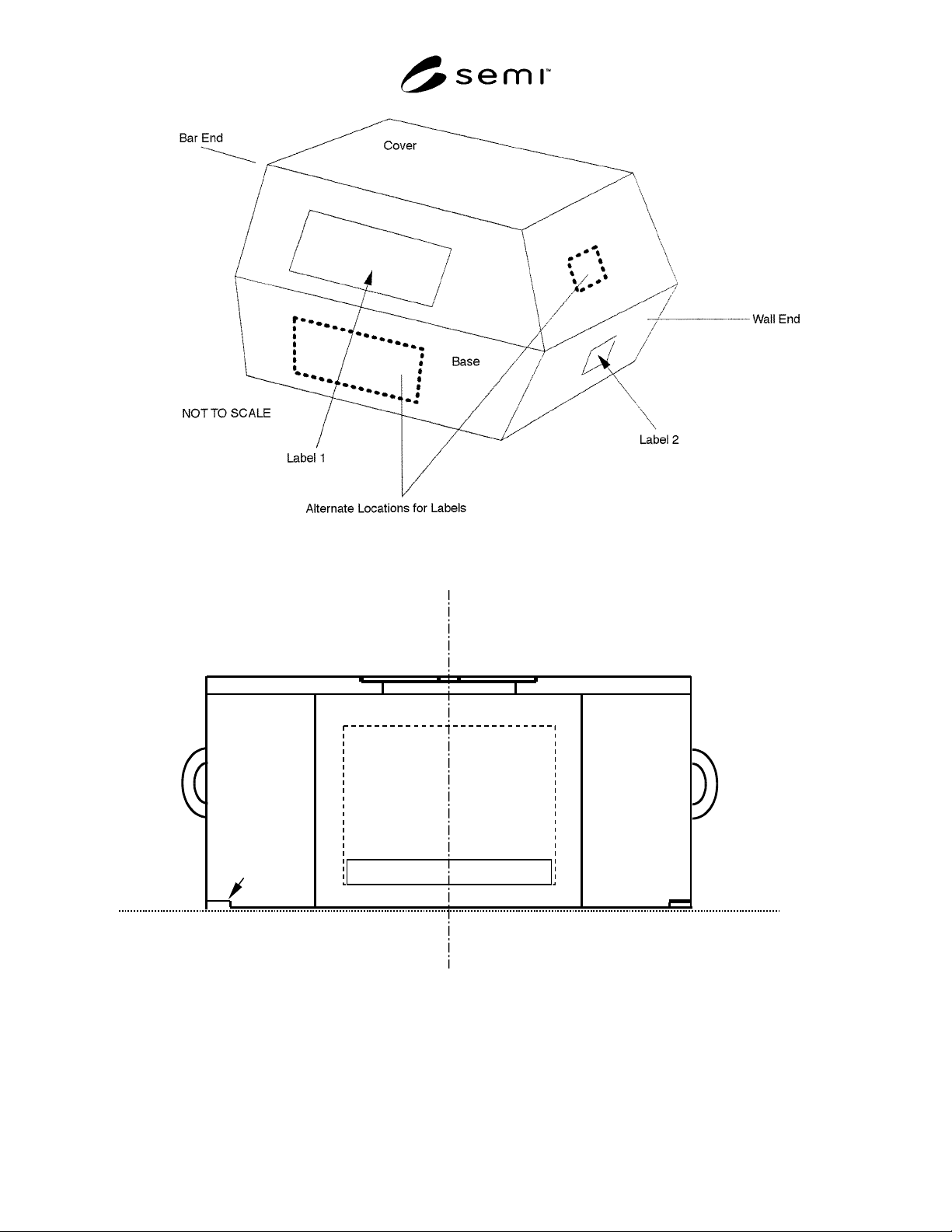
Figure 7
Recommended and Alternative Locations for Labels on Wafer Boxes for
Use with Wafers of 100 to 200 mm Diameter
Bilateral Datum Plane
Bottom Rail
Human Handle
(
o
p
tional
)
Horizontal Datum Plane of
Box Nest or Load Port
Rear Surface
Label Area
Preferred Label Location
Figure 8a
300 mm FOSB Rear Surface Label Locations
SEMI T3-0302 © SEMI 1995, 2002 15
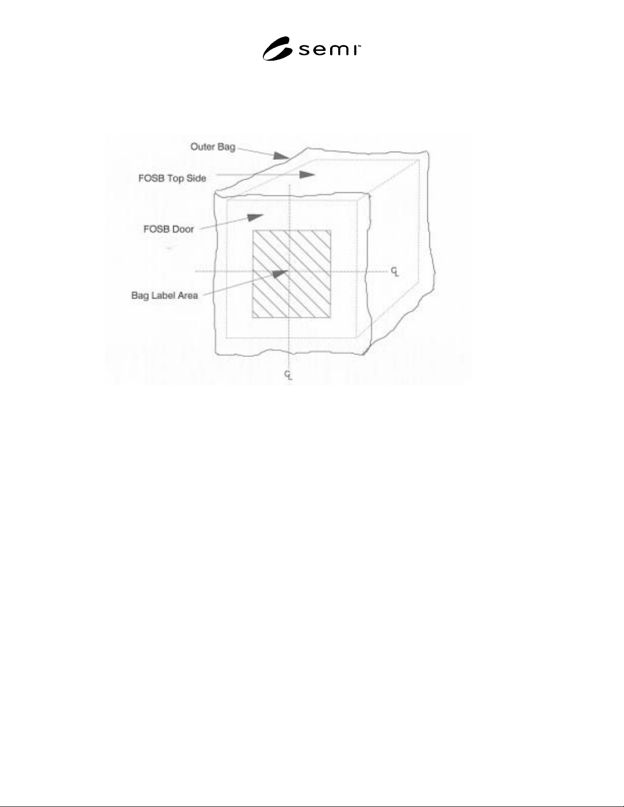
Figure 8b
FOSB Associated Outer Bag Label Location
NOTICE: SEMI makes no warranties or representations as to the suitability of the standards set forth herein for any
particular application. The determination of the suitability of the standard is solely the responsibility of the user.
Users are cautioned to refer to manufacturer' s instructions, product labels, product data sheets, and other relevant
literature, respecting any materials or equipment mentioned herein. These standards are subject to change without
notice.
By publication of this standard, Semiconductor Equipment and Materials International (SEMI) takes no position
respecting the validity of any patent rights or copyrights asserted in connection with any items mentioned in this
standard. Users of this standard are expressly advised that determination of any such patent rights or copyrights, and
the risk of infringement of such rights are entirely their own responsibility.

SEMI T3-0302 © SEMI 1995, 2002 16
RELATED INFORMATION 1
MODIFIED DATE FORMAT
NOTE: This related information is not an official part of SEMI T3 and was derived from information developed by the T3
Revision task force of the N.A. Traceability committee during revision of the standard. This related information was approved
for publication in June 1997 after full letter ballot and approval by the NA Regional Standards Committee.
R1-1 Alternative Labeling Date Format
R1-1.1 By agreement between supplier and customer, the labeling date may be in the format of YYYYMMDD.
The data identifier “6D” should be used when the year is indicated by four characters. This adds three characters to
the information printed on the label, two additional date characters and the second character in the data identifier.
There is space available on the minimum size label when using the two-dimensional data matrix symbol or the
optional Code 128 bar code. Three additional characters added to the Code 39 bar code will not fit on the minimum
size label unless the Lot Number is reduced to 13 characters.
NOTICE: SEMI makes no warranties or representations as to the suitability of the standards set forth herein for any
particular application. The determination of the suitability of the standard is solely the responsibility of the user.
Users are cautioned to refer to manufacturer' s instructions, product labels, product data sheets, and other relevant
literature, respecting any materials or equipment mentioned herein. These standards are subject to change without
notice.
By publication of this standard, Semiconductor Equipment and Materials International (SEMI) takes no position
respecting the validity of any patent rights or copyrights asserted in connection with any items mentioned in this
standard. Users of this standard are expressly advised that determination of any such patent rights or copyrights, and
the risk of infringement of such rights are entirely their own responsibility.
Copyright by SEMI ® (Semiconductor Equipment and Materials
International), 3081 Zanker Road, San Jose, CA 95134. Reproduction o
f
the contents in whole or in part is forbidden, without express writte
n
consent of SEMI.