semi合集-English.pdf - 第7906页
SEMI T14-1104 © SEMI 2004 3 5.2.3 The length of each dot mark along the surface of the article to be marked sh ould be 6.0 µ m + 1 0% – 20%. (As shown in Fi gure 3.) 5.3 Border R ows and Columns 5.3.1 One border row and …

SEMI T14-1104 © SEMI 2004 2
4 Terminology
4.1 Definitions
4.1.1 alignment bar, of a data matrix code symbol — a solid line of contiguous filled cells abutting a line of
alternately filled and empty cells [ISO/IEC ISS 16022].
4.1.2 binary values — a protrusion dot in the wafer surface indicates the binary value 1. The absence of a dot, or a
smooth surface surrounding a cell center point indicates the binary value 0.
4.1.3 border column — the outermost column of a data matrix code symbol. This column is a portion of the finder
pattern.
4.1.4 border row — the outermost row of a data matrix code symbol. This row is a portion of the finder pattern.
4.1.5 cell center point, of an array — the point at which the centerline of a row intersects the centerline of a
column.
4.1.6 cell, of a data matrix code symbol — the area within which a dot may be placed to indicate a binary value.
4.1.7 cell spacing, of an array — the (equal) vertical or horizontal distance between the cell center points of
contiguous cells.
4.1.8 center line, of a row or column — the line positioned parallel to, and spaced equally between, the boundary
lines of the row or column.
4.1.9 central area, of a cell — the area enclosed by a circle centered at the cell center point; used by code readers to
sense the binary value of the cell.
4.1.10 data matrix code symbol — a two-dimensional array of square cells arranged in contiguous rows and
columns. In certain ECC200 symbols, data regions are separated by alignment patterns. The data region is
surrounded by a finder pattern [ISO/IEC ISS 16022].
4.1.11 finder pattern, of a data matrix code symbol — a perimeter to the data region. Two adjacent sides contain
dots in every cell; these are used primarily to define physical size, orientation and symbol distortion. The two
opposite sides are made up of cells containing dots in alternate cells [ISO/IEC ISS 16022].
4.1.12 Micro ID — Micro ID consists of the data matrix code symbol, which is formed with some protruding marks
on the silicon wafers.
4.1.13 protrusion dot — a locally protruded region with a reflectance which differs from that of the surrounding
surface.
NOTE 1: To assure reading efficiency, a minimum contrast of 30% is required between the reflectance value of a dot and the
surrounding wafer surface. Various densitometers can provide such measurements nondestructively.
4.1.14 protrusion dot misalignment, within a cell — the distance between the physical center point of a protrusion
dot and the cell center point.
5 Requirements
5.1 Shape and Size of the Data Matrix Code Symbol
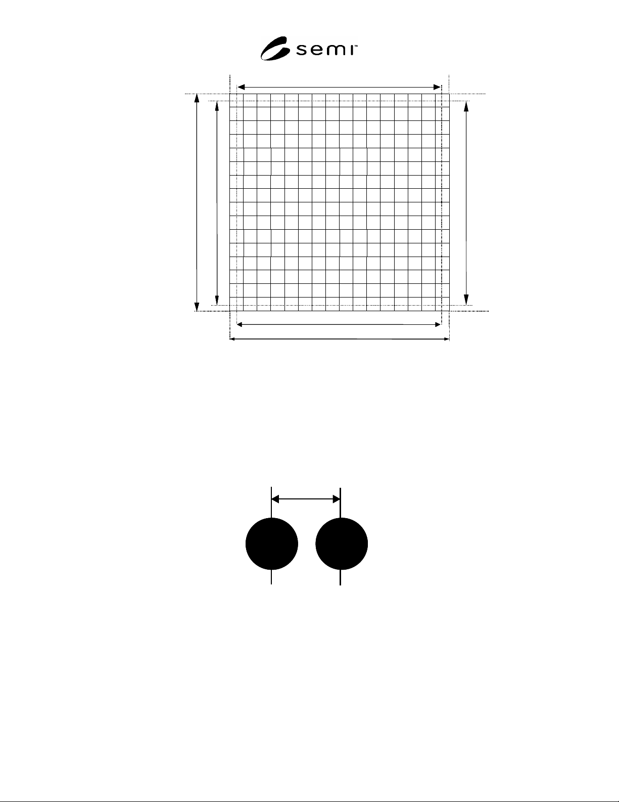
5.1.1 Each square data matrix code symbol shall be composed of an array of 16 rows and 16 columns as defined in
ISO/IEC ISS 16022. (As shown in Figure 1.)
5.1.2 Cell spacing shall be 6.25 µm, center to center. (As shown in Figure 2.)
5.2 Shape and Size of the Microdot Mark
5.2.1 A microdot mark is formed by laser irradiation and consists of a single dot mark on each laser-irradiated
point.
5.2.2 The mark has a single protrusion, which includes a concave portion provided around the protrusion and lower
than a surface of the wafer and whose center potion protrudes upward so as to be higher than the surface of the
wafer.

SEMI T14-1104 © SEMI 2004 3
5.2.3 The length of each dot mark along the surface of the article to be marked should be 6.0 µm + 10% – 20%. (As
shown in Figure 3.)
5.3 Border Rows and Columns
5.3.1 One border row and one border column shall contain a dot in each cell. These are identified as the primary
border row and the primary border column. They are used by the code reader to determine the orientation of the
matrix.
5.3.2 The opposing (secondary) border row and column shall contain dots in alternating cells.
5.3.3 The reference point shall be the physical center point of corner cell common to the primary border row and
the primary border column. (As shown in Figure 4.)
5.3.4 The maximum dot misalignment within a cell is 1.4 µm. This ensures that a minimum size dot covers a cell
central area of radius 1 µm.
5.4 Content of the Data Matrix Code Symbol
5.4.1 Each square data matrix code symbol shall contain 16 message characters, together with the error checking
and correcting (ECC200) code characters, encoded in accordance with ISO/IEC ISS 16022.
5.4.2 The message characters shall include the following: A–Z, 0–9, and dash (–).
5.5 Location of the Data Matrix Code Symbol
5.5.1 With the wafer positioned front surface up and with the primary fiducial (notch) toward the operator, the
origin of the data matrix code symbol shall be located as specified below. (As shown in Figure 5.)
5.5.1.1 Circular position — the reference point shall be located along the perimeter by 3.0 ± 0.1° counterclockwise
from the axis of the notch fiducial bisector. (As shown in Figure 5.)
5.5.1.2 Radial position — the mark position of Micro ID is decided by the responsibility of Device Manufacturers
on the bevel area where the Micro ID is survived even after the CMP processing and the backside grind. (Related
Information in Figure R1-2.)
5.5.2 The primary border row of the data matrix code symbol shall be placed toward the periphery of the wafers,
and the primary border column of the data matrix code symbol shall be placed toward the center of the wafers,
originating from the reference point.
SEMI T14-1104 © SEMI 2004 4
Nominal Dimensions (µm)
R1 = 92.00 ± 6%
C2 = 98.00 ± 6% R2 = 98.00 ± 6%
C1 = 92.00 ± 6%
16
cells per row
C1
C2
R1
R2
16
cells per
column
C
L
C
L
C
L
C
L
16
cells per row
C1
C2
R1
R2
16
cells per
column
C
L
C
L
C
L
C
L
C
L
C
L
C
L
C
L
Figure 1
Data Matrix Field Dimensions
ECC200 - 16 rows × 16 columns
6.25 µ m
6.25
µ
m
Figure 2
Cell Spacing