semi合集-English.pdf - 第6261页
SEMI G51-90 © SEMI 1990 3 measuring corner to corner: Overall maximum not to exceed a total of 0.102 m m (0.004"). 6.6 Pits and Sl ug Mar ks 6.6.1 Within t he functional area and o n external leads, no slug marks an…
SEMI G51-90 © SEMI 1990 2
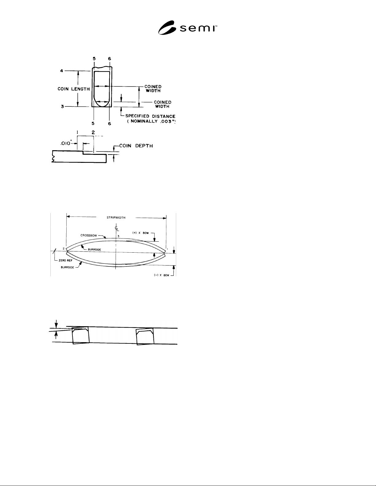
Figure 3
Coined Area
crossbow — Transverse bowing of the leadframe (see
Figure 4).
Figure 4
Crossbow
lead twist — Angular rotation of bonding fingers (see
Figure 5).
Figure 5
Lead Twist
pits — Shallow surface depressions or craters in the
leadframe material.
true position circle — That circle with its center
positioned at the center of the coined lead defines the
design position of the lead tip.
4 Ordering Information
Purchasing orders for leadframes for plastic Molded
Quad Flat Pack packages furnished to this specification
shall include the following items:
4.1 Drawing number and revision level.
4.2 Material alloy specification.
4.3 Lead count, and confirming number of units per
strip.
4.4 Requirement for material certification.
4.5 Leadframe plating specifications.
5 Dimensions
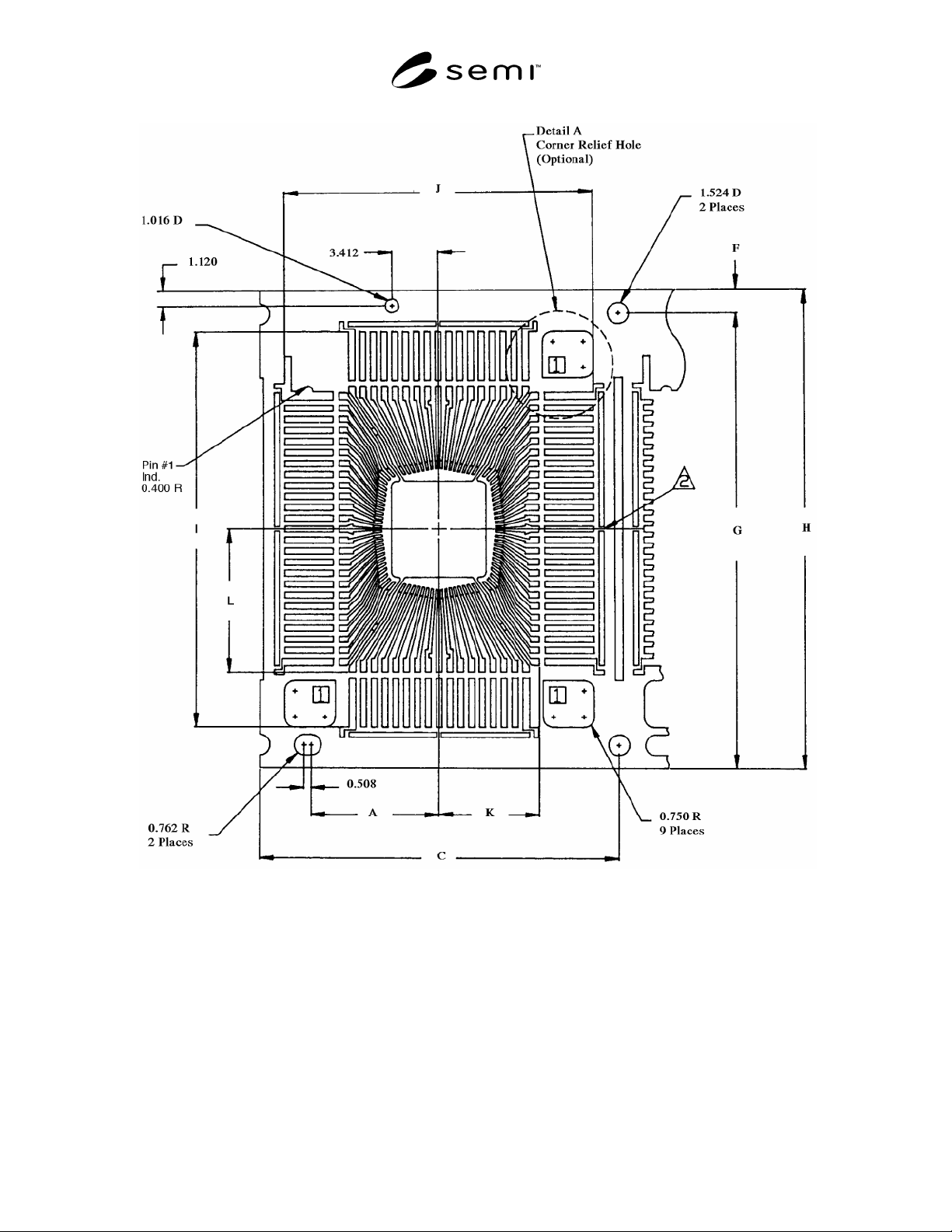
5.1 Tables I, II.
5.2 See Figure 6 and Detail A.
6 Defect Limits and Parameters
(To measure, see SEMI G10).
6.1 Lead Tip Width
6.1.1 Minimum Lead Tip Width — Shall be as agreed
to between supplier and purchaser.
6.1.2 Minimum Flat Wire Bonding Area — 80% of
nominal lead width and 0.635 mm (0.025") in length.
NOTE: This applies to stamped frames; percent of nominal
lead width for etched frames must be determined between
purchaser and supplier and is dependent on etch tolerances.
6.2 Coining and Metal Clearance
6.2.1 If coined, maximum depth = 30% material
thickness. Minimum depth as agreed to between
supplier and purchaser.
6.2.2 On stamped frames, dimensions shown on
drawings are before coining.
6.2.3 Metal-to-Metal Clearance — Shall be as agreed
to between supplier and purchaser.
6.3 Lead Twist — Shall not exceed 3.5 or 0.015 mm
(0.0006") per 0.254 mm (0.010") of lead width.
6.4 Burrs — Shall be firmly attached and able to
withstand a probe force of 10 grams. All burrs vertical
and horizontal in any location shall not exceed 0.0254
mm (0.001").
6.5 Die Pad Tilt and Flatness — (See specification
SEMI G10 for measurement method).
6.5.1 Tilt — 0.025 mm (0.001") maximum per 2.54
mm (0.100") of length or width in the undepressed
state, and 0.051 mm (0.002") maximum per 4.06 mm
(0.160") of length or width in the depressed state, when

SEMI G51-90 © SEMI 19903
measuring corner to corner: Overall maximum not to
exceed a total of 0.102 mm (0.004").
6.6 Pits and Slug Marks
6.6.1 Within the functional area and on external leads,
no slug marks and pits shall exceed 0.008 mm
(0.0003") in depth and 0.0127 mm (0.0005") in length.
NOTE: There is a question regarding the ability of material
suppliers to meet this specification. Revision of this
specification is under review.
6.6.2 They shall not exceed 0.0254 mm (0.001") in
depth and 0.051 mm (0.002") in length in nonfunctional
areas.
6.7 Material Thickness — 0.150 mm (0.0059") ±
0.005 mm (0.0002") for all lead counts.
6.8 Internal Position Tolerance — The centerline of
all leadframe features must be within T.P.T. 0.051 mm
(0.002") relative to centerline of pilot holes on rail.
6.9 Lead Tip Coplanarity — Shall be within the
following tolerances as measured relative to the Z
datum plane located at the center of the die attach pad
or per SEMI G10 measurement method:
44–52 lead counts: ± 0.10 mm (0.004")
64–100 lead counts: ± 0.15 mm (0.006")
120–232 lead counts: ± 0.20 mm (0.008")
6.10 Progression
6.10.1 Single progression of one frame is T.P.T. 0.051
mm (0.002").
6.10.2 Accumulated progression tolerance over the
strip length (measured from pitch line tooling hole to
pitch line tooling hole, across the strip length minus the
two end units) is within T.P.T. of 0.102 mm (0.004").
6.11 Strip Cut Off Location — Shall be within T.P.T.
0.154 mm (0.006") of nominal strip length.
6.12 Strip Width Tolerance — T.P.T. 0.102 mm
(0.004").
6.13 Camber — Shall not exceed 0.051 mm (0.002")
over the nominal strip length.
6.14 Coil Set — Maximum of 0.508 mm (0.020") over
the nominal strip length. This does not include material
thickness.
6.15 Cross Bow — Shall not exceed 0.7% of the
nominal strip width.
6.16 External nominal lead width dimension will be as
follows for each respective lead pitch requirement:
1.0 mm lead pitch: 0.4 mm (stamped or etched)
8 mm lead pitch: 35 mm (stamped or etched)
65 mm lead pitch: 0.27 mm (etched)
3 mm (stamped)
Please note that specific etching and stamping
tolerances associated with lead widths are to be
negotiated and specified between purchaser and
supplier.
PLEASE NOTE: THESE SPECIFICATION
DIMENSIONS AND CRITICAL TOLERANCES,
UNLESS OTHERWISE NOTED, APPLY TO ALL
ALLOY 42, COPPER ALLOY, ETCHED AND
STAMPED LEADFRAME MATERIALS.
7 Sampling
A sampling plan and buy-off procedure to determine
compliance to the requirements of Sections 5 and 6 and
other relevant specifications shall be determined
between vendor and customer.
8 Packaging and Marking
8.1 Packaging — Tooling must be packed in
containers designed and constructed to provide
protection against normal transportation damage risks
and spillage. The container will offer protection from
contamination and exposure to moisture.
8.2 Marking — The following details shall be noted
on the packing slip:
Quantity and Description
Vendor Lot Numbers
Vendor Part Number
Customer Drawing Numbers
Customer Part Number
Shipping Date
Customer P.O. Number
SEMI G51-90 © SEMI 1990 4
Figure 6
Frame Unit
1. Corner relief holes are optional features only. Gating may require their exclusion.
2. Lead counts 100 and below have only 1 support tab per each frame expansion slot. Lead counts 120 and above
have 3 support tabs evenly spaced for each frame expansion slot. Tabs are to be placed opposite the space.