semi合集-English.pdf - 第7596页
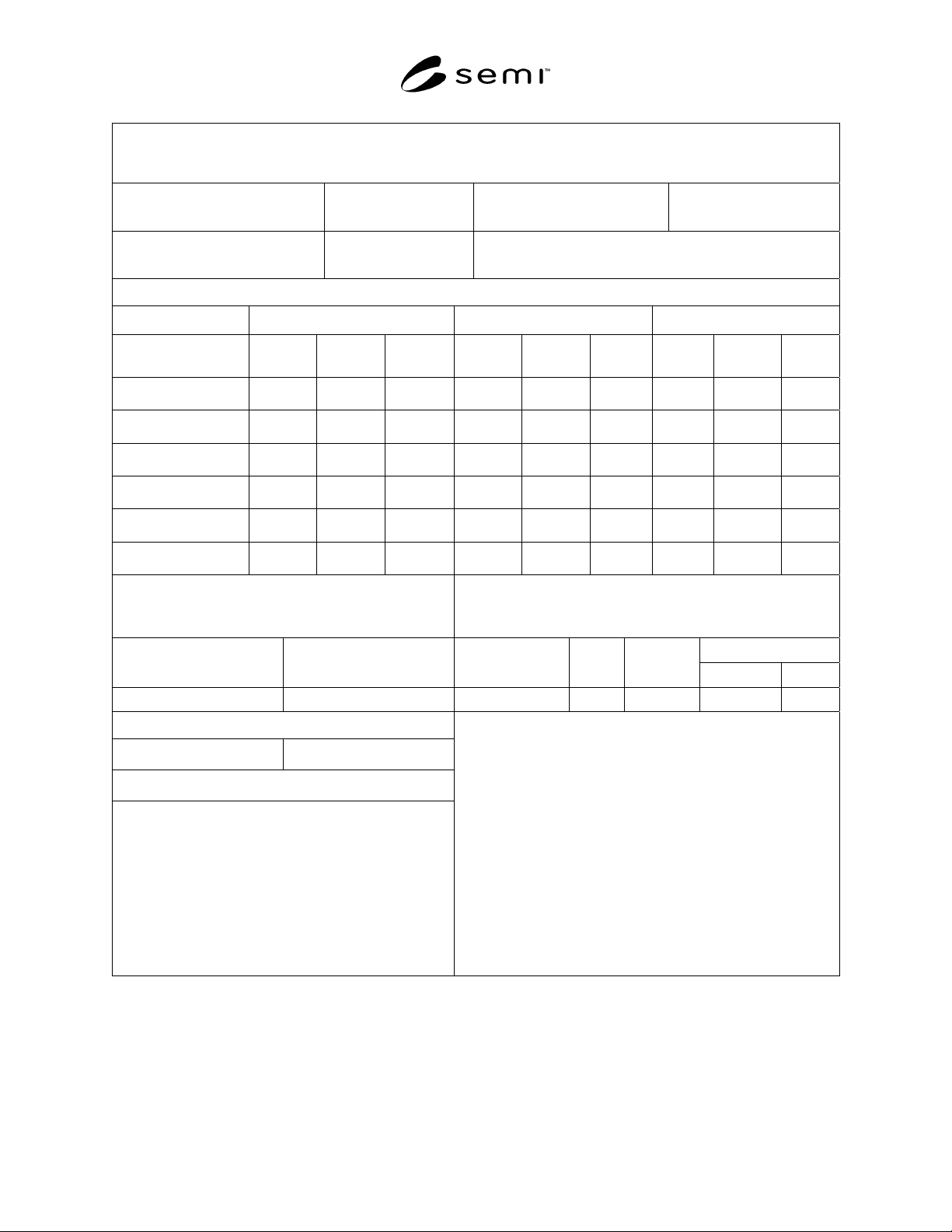
SEMI MF2166-0304 © SEMI 2004 9 Special Reference Wafer Calibra tion Data Sheet For Non-Contact Dielectric Charac terization System System Supplier: System Model #: System Software Rev: Test Date: Calibration Organization…
SEMI MF2166-0304 © SEMI 2004 8
Special Reference Wafer Calibration Data Sheet For
Non-Contact Dielectric Characterization System
System Supplier: System Model #:
System Software Rev: Test Date:
Calibration Organization
Operator ID Method A — Point Source Corona [ ]
Method B — Line Source Corona [ ]
Measurement Data Statistics
Mean
Std Dev (1 sigma) % Std Dev (1S%)
Location
Parameter
(0,0) (-40,40) (40,-40) (0,0) (-40,40)
(40,-40)
(0,0) (-40,40) (40,-40)
V
surf
(V) (Method A)
V
cpd,
(V) (Method B )
T
ox
(nm)
V
fb
(V)
Q
eff
(×10
11
charge/ cm
2
)
D
it
(×10
11
charge/ cm
2
)
Q
m
(× 10
11
charge/ cm
2
)
Environmental Data
Special Reference Wafer Used
Calibration Dates
Temperature
____ [ ]°F [ ]°C
Relative Humidity Serial Number Mfg.
Wafer
Dia.
Last Next
Equipment Performance Summary
In Tolerance [ ] Out of Tolerance [ ]
Repair Required Yes [ ] No [ ]
Comments
Figure 1
Example Data Sheet for Methods A and B
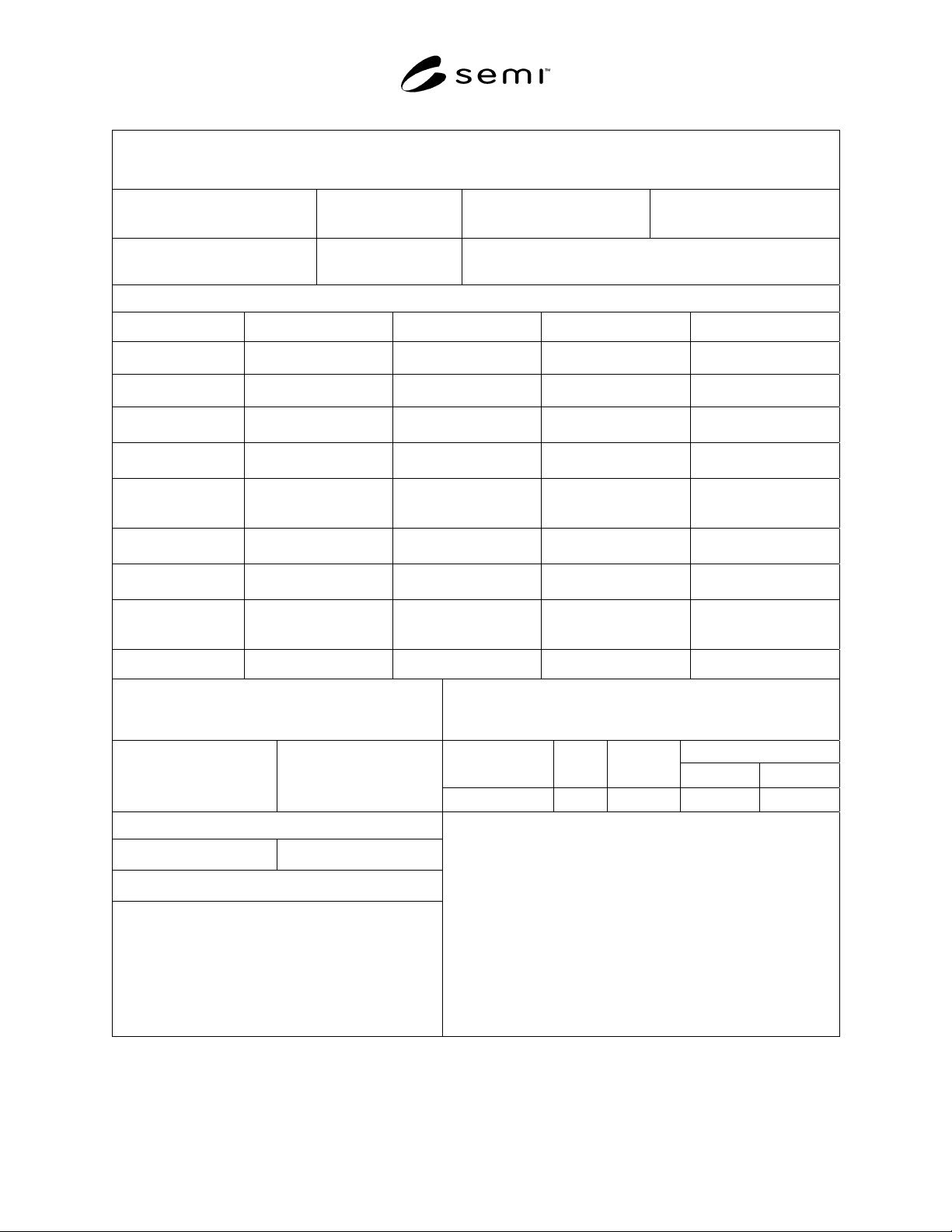
SEMI MF2166-0304 © SEMI 2004 9
Special Reference Wafer Calibration Data Sheet For
Non-Contact Dielectric Characterization System
System Supplier: System Model #:
System Software Rev: Test Date:
Calibration Organization
Operator ID Method C — Line Source Corona [ ]
Measurement Data Statistics
Parameter
Mean
Std Dev (1 sigma) Minimum Maximum
V
cpd,
(V)
Corona Voltage per
Sweep
(−) CTS Voltage
(−) CTS Time
(−) CTS
Temperature
(+) CTS Voltage
(+) CTS Time
(+) CTS
Temperature
Q
m
(× 10
11
charge/ cm
2
)
Environmental Data
Special Reference Wafer Used
Calibration Dates
Serial Number Mfg.
Wafer
Dia.
Last Next
Temperature
_____ [ ]°F____ [ ]°C
Relative Humidity
Equipment Performance Summary
In Tolerance [ ] Out of Tolerance [ ]
Repair Required Yes [ ] No [ ]
Comments
Figure 2
Example Data Sheet for Method C
SEMI MF2166-0304 © SEMI 2004 10
RELATED INFORMATION 1
CORONA SUBSYSTEMS
NOTICE: This related information is not an official part of SEMI MF2166. It was developed during the original
development of the document. This related information was approved for publication by full letter ballot on October
16, 2003.
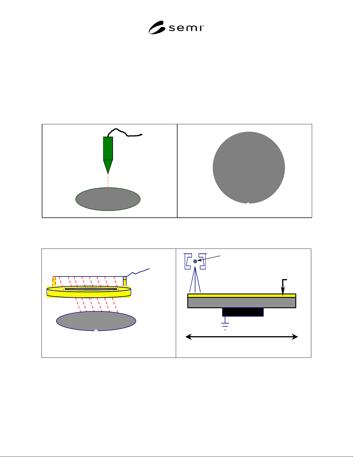
R1-1.1 Two types of coronas are used in NCDCSs:
R1-1.2 Point Source Corona — This corona type
applies charge at discrete locations on the wafer
surface. The area of the corona is defined by a mask.
(See Figure R1-1.)
R1-1.3 Line Corona — In this corona, a wire applies a
charge uniformly across the entire wafer. The charge
level is applied in increments that cause a V
cpd
change
of between 0.3 and 0.6 V. (See Figure R1-2.)
High
Voltage
Wafer
Linear Sam
p
lin
g
+
+
+
Figure R1-1
Point Corona – Method A
High
Voltage
Corona Wire
Wafer
High Voltage
Corona Wire
x
-motion
A
rea Scannin
g
Silicon
Chuc
k
Oxide
+ + + + + + + + + + +
Figure R1-2
Wire Corona – Method B and C