semi合集-English.pdf - 第6277页
SEMI G54-93 © SEMI 1993 5 Figure 5 Mis m at ch Figure 6 Offset Figure 7 Package Warp age NOTICE : These standards do n ot purport to address safety issues, if any, as sociated with their use. It is the responsibility of …
SEMI G54-93 © SEMI 1993 4
8 Packaging and Marking
8.1 Packaging — Tooling must be packed in
containers designed and constructed to provide
protection against normal transportation damage risks
and spillage. The container will offer protection from
contamination and exposure to moisture. Tools may be
coated with a suitable rust inhibitor as agreed between
vendor and customer.
8.2
Marking — The following details shall be noted
on the packing slip:
Vendor Part Number
Customer Part Number
Shipping Date
Customer P.O. Number
Shipment Items
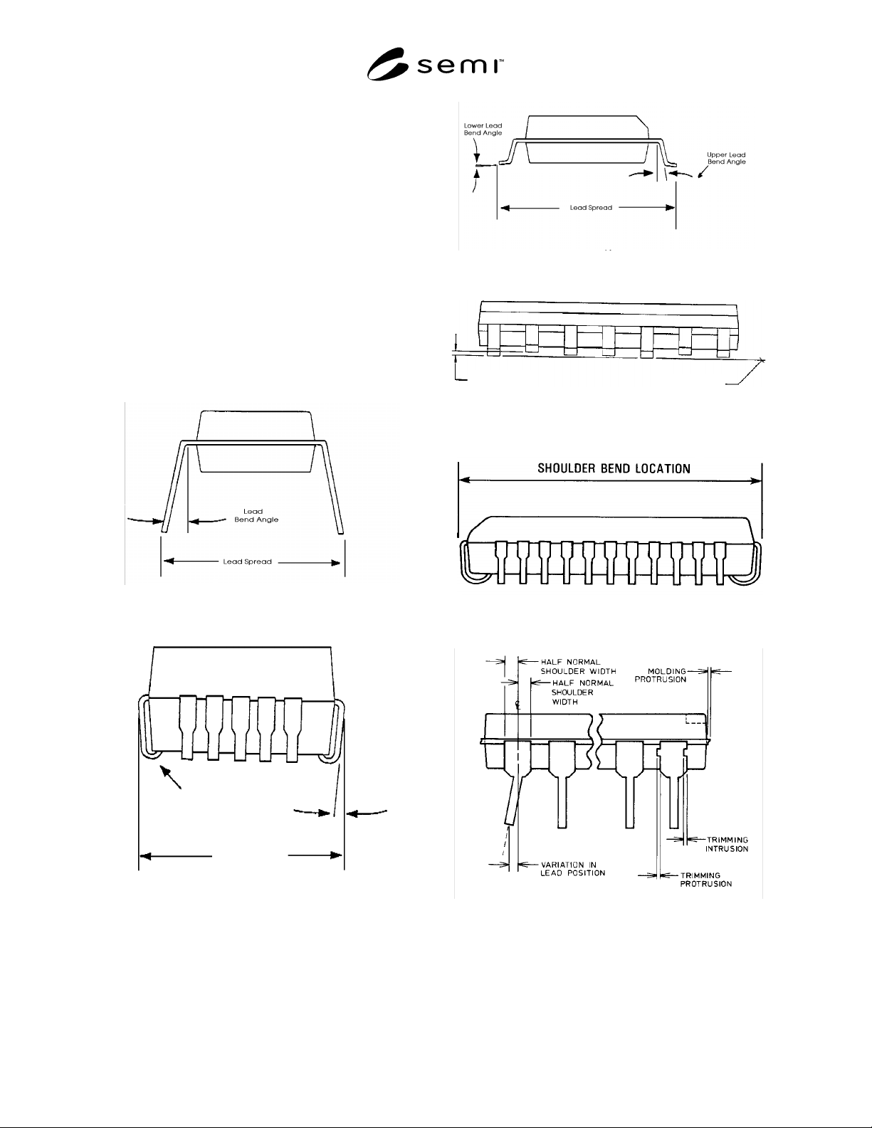
Figure 1A
PDIP Package
Foot
Radius
Lead
Bend Angle
Lead Spread
Figure 1B
PLCC Package
Figure 1C
SOIC and PQFP Packages
Vertical Lead
Position
Reference Plane
Figure 2
Lead Co-planarity
Figure 3
Shoulder Bend Location
Figure 4
Parting Line Protrusion, Lead Sweep and Lead
Shoulder Protrusions and Intrusions
SEMI G54-93 © SEMI 19935
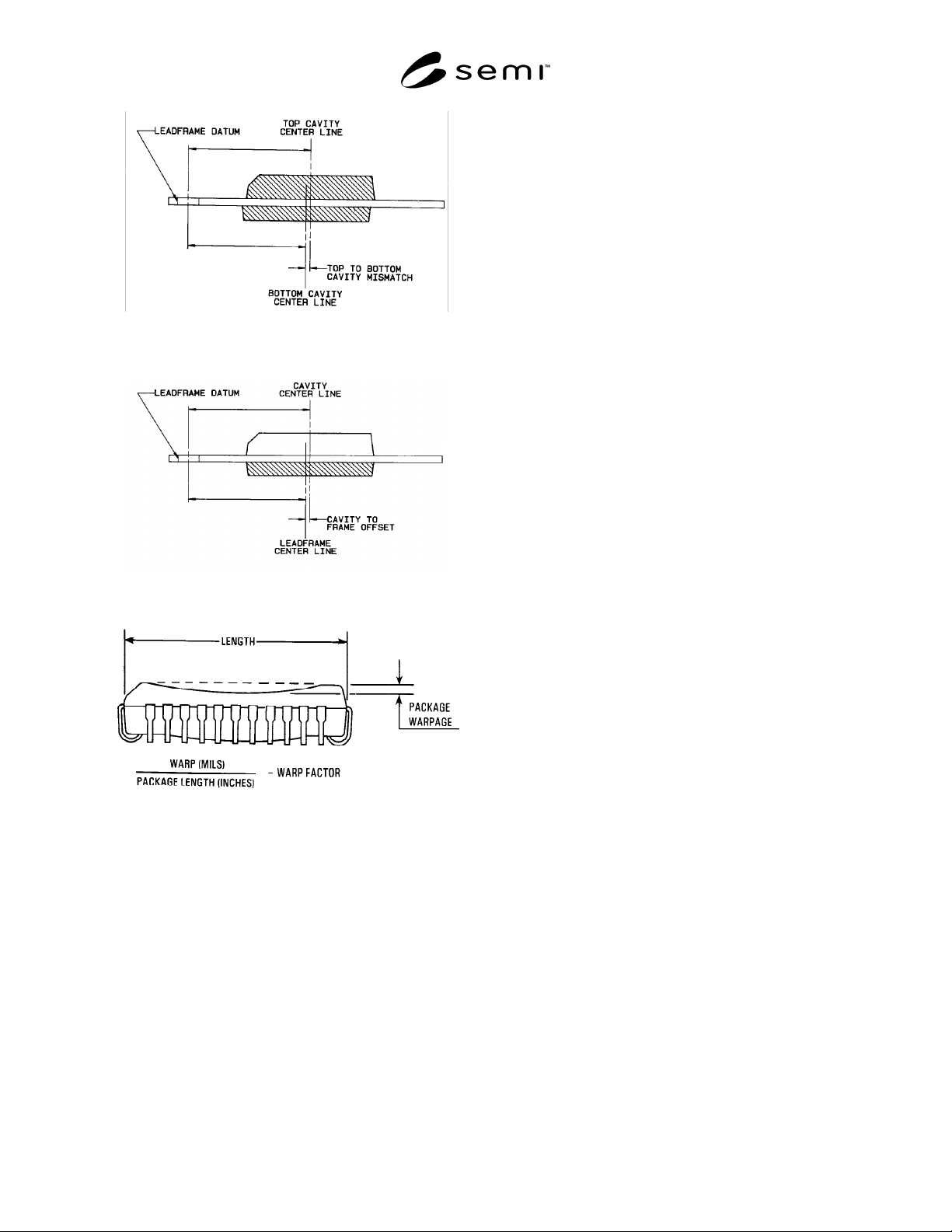
Figure 5
Mismatch
Figure 6
Offset
Figure 7
Package Warpage
NOTICE: These standards do not purport to address
safety issues, if any, associated with their use. It is the
responsibility of the user of these standards to establish
appropriate safety and health practices and determine
the applicability of regulatory limitations prior to use.
SEMI makes no warranties or representations as to the
suitability of the standards set forth herein for any
particular application. The determination of the
suitability of the standard is solely the responsibility of
the user. Users are cautioned to refer to manufacturer’s
instructions, product labels, product data sheets, and
other relevant literature respecting any materials
mentioned herein. These standards are subject to
change without notice.
The user’s attention is called to the possibility that
compliance with this standard may require use of
copyrighted material or of an invention covered by
patent rights. By publication of this standard, SEMI
takes no position respecting the validity of any patent
rights or copyrights asserted in connection with any
item mentioned in this standard. Users of this standard
are expressly advised that determination of any such
patent rights or copyrights, and the risk of infringement
of such rights, are entirely their responsibility.
Copyright by SEMI® (Semiconductor Equipment and Materials
International), 3081 Zanker Road, San Jose, CA 95134. Reproduction o
f
the contents in whole or in part is forbidden without express written
consent of SEMI.

SEMI G55-93 © SEMI 1993, 2004 1
SEMI G55-93 (Reapproved 1104)
TEST METHOD FOR MEASUREMENT OF SILVER PLATING
BRIGHTNESS
This test method was technically reapproved by the Global Assembly & Packaging Committee and is the
direct responsibility of the Japanese Packaging Committee. Current edition approved by the Japanese
Regional Standards Committee on July 23, 2004. Initially available at www.semi.org September 2004; to be
published November 2004. Originally published in 1993.
1 Preface
1.1 Use — This test may be used for process control
and outgoing inspection at the supplier or by the user
for incoming inspection.
2 Scope
2.1 This method describes the standard method for
measuring the brightness of silver plating on
semiconductor leadframes.
NOTE 1: This method determines quantitative measures
which are not related directly to the traditional “Dull,” “Semi-
Bright” and “Bright” descriptors for silver plating.
NOTICE: This standard does not purport to address
safety issues, if any, associated with its use. It is the
responsibility of the users of this standard to establish
appropriate safety and health practices and determine
the applicability of regulatory or other limitations prior
to use.
3 Referenced Standards
3.1 SEMI Standard
SEMI G21 — Specification for Plating Integrated
Circuit Leadframes
3.2 JIS Specifications
1
JIS H8621 — Electroplated Coatings of Silver for
Engineering Use
JIS Z8722 — Method of Measurement for Color of
Reflecting or Transmitting Objects
JIS Z8741 — Method of Measurement for Specular
Glossiness
3.3 Military and Federal Specifications
2
QQ-S-365 — General Requirements for Electro-
deposited Silver Plating
1 Japanese Industrial Standards, Available through the Japanese
Standards Association, 1-24, Akasaka 4-Chome, Minato-ku, Tokyo
107-8440, Japan. Telephone: 81.3.3583.8005; Fax: 81.3.3586.2014,
Website: www.jsa.or.jp
2 United States Military Standards, Available through the Naval
Publications and Forms Center, 5801 Tabor Avenue, Philadelphia,
PA 19120-5099, USA. Telephone: 215.697.3321
NOTICE: Unless otherwise indicated, all documents
cited shall be the latest published versions.
4 Significance
4.1 Brightness values indicate surface roughness for
given plating conditions. Surface roughness affects the
wettability of resinous die attach processes on
leadframes. If the surface is too smooth, poor wetting
may occur which results in low die share strength
values.
4.2 Brightness variations may also affect the ability of
the pattern recognition systems used on assembly
equipment to recognize the set points.
5 Summary of Method
5.1 The method is based on the use of a GAM
Densitometer. This method is chosen as the standard
because of the small measurement area requirements
and the high accuracy of the method for typical silver
plating brightness used on leadframes.
5.1.1 This method is based on the measurement of the
reflectance of light at 45° from a surface illuminated
from a light source perpendicular to the surface. This
value of Reflectance (R) gives a Density Value (D)
based on the following formula:
D = log 1/R
Density is a measure of the Brightness.
6 Interferences
6.1 Surface Finish
6.1.1 Brightness values depend on surface roughness.
A rough surface shows a low brightness value when
compared to a smooth surface. Variable plating
conditions, such as the addition of brighteners to the
plating solution, may give brightness results, which are
not comparable for the acceptance of plated leadframes.
6.1.2 Scratches and other flaws in the surface will
affect reflectance.
6.2 Storage Time and Conditions
6.2.1 Figure 1 shows the brightness results for
leadframes subjected to indoor, atmospheric storage for