semi合集-English.pdf - 第6537页
SEMI G81-0703 © SEMI 2000, 2003 12 APPENDIX 3 TRAY MAP ORIENTATION NOTICE : The material in this appendix is an official part of SEMI G81 and was approved by full letter ballot procedures on August 27, 2001. A3-1 This ap…
SEMI G81-0703 © SEMI 2000, 2003 11
APPENDIX 2
STRIP MAP
NOTICE: The material in this appendix is an official part of SEMI G81 and was approved by full letter ballot
procedures on August 27, 2001.
A2-1 This appendix shows how the map data items may be applied to strips as well as some additional information
specific to this substrate type.
A2-2 The StripID shall follow the SEMI T9 specification, when applicable, or may be user definable by the factory.
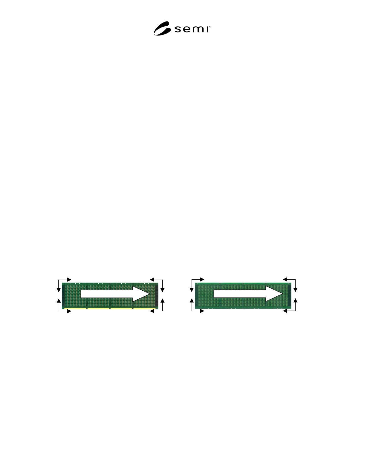
A2-3 For any given process there must be a way to ensure correct orientation of the strip. The end user is
responsible for providing a master manufacturing drawing showing the top side of the strip. This drawing must show
any special markings or patterns that are needed to reliably flip and rotate a physical strip until it is oriented the
same as the drawing. Figure A2-1 defines what is meant by top side and hence bottom side. It also defines what is
meant by upper, lower and left and right.
A2-4 Each strip type will have a factory defined value for OriginLocation. This is the origin reference for the row 1,
column 1 location on the strip. The factory origin, OriginLocation is selected as one of four corners by the factory
host system. The row and column index will be referenced from the selected reference. This information will be
provided to the equipment by the host in each strip map download scenario.
1 = Upper right (UR) top side
2 = Upper left (UL) top side
3 = Lower left (LL) top side
4 = Lower right (LR) top side
6 = Upper right (UR) bottom side
7 = Upper left (UL) bottom side
8 = Lower left (LL) bottom side
9 = Lower right (LR) bottom side
Row Row
Column
Row Row
Column Column
Column
Std Process Direction
12
34
Top Side
Row Row
Column
Row Row
Column Column
Column
Std Process Direction
67
89
Bottom Side
Figure A2-1
Factory Origin Settings
SEMI G81-0703 © SEMI 2000, 2003 12
APPENDIX 3
TRAY MAP ORIENTATION
NOTICE: The material in this appendix is an official part of SEMI G81 and was approved by full letter ballot
procedures on August 27, 2001.
A3-1 This appendix shows how the map data items may be applied to JEDEC trays as well as some additional
information specific to this substrate type.
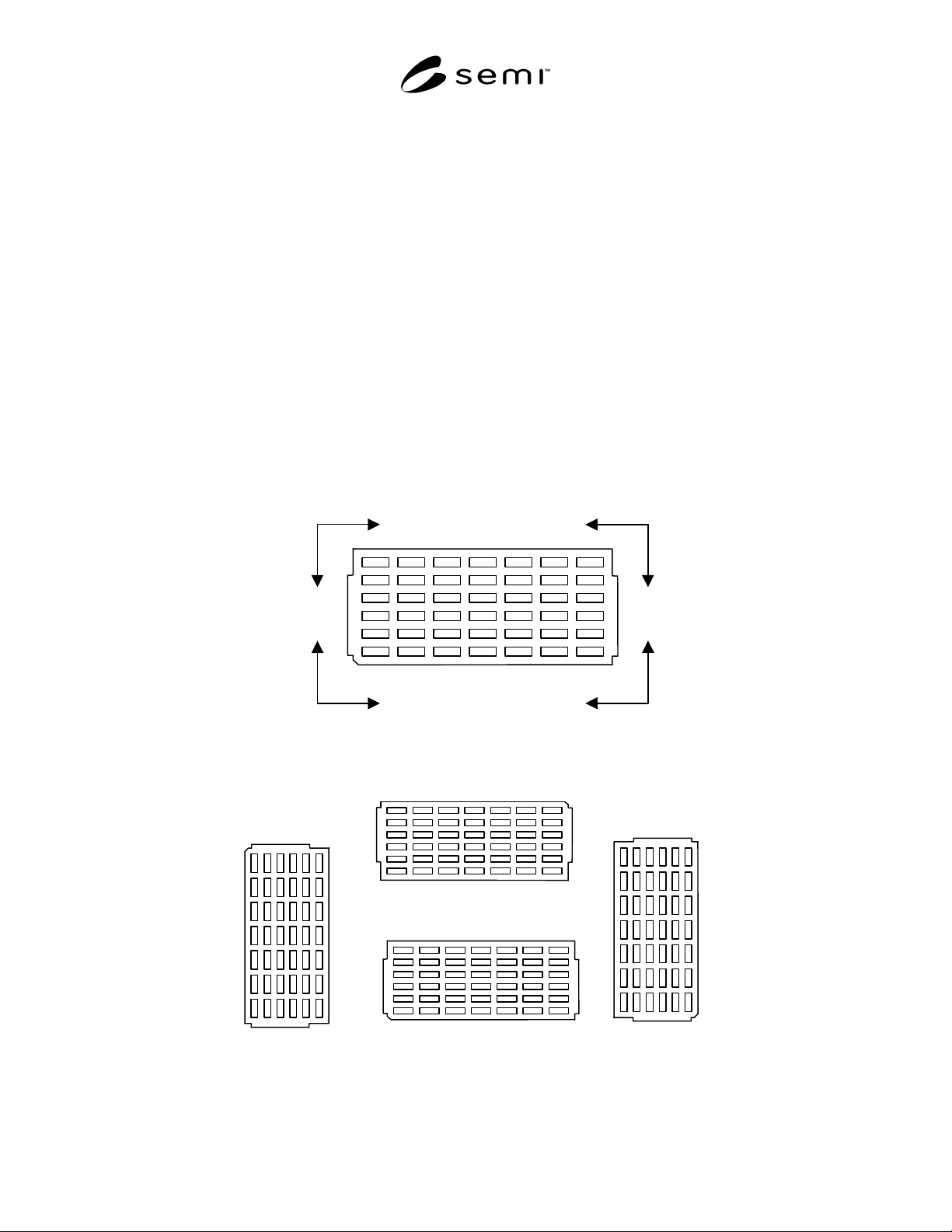
A3-2 The X-axis (Column) is assigned to the long axis of the JEDEC tray; the Y-axis (Row) is assigned to the short
axis of the tray. This corresponds to Cartesian coordinate “1” (in this way all coordinate positions can be expressed
in positive integer values). For the origin of the tray, the pocket nearest the bevel (at the bottom left corner of the
tray in Figure A3-1 below) is defined as coordinate location 0,0. (Row/Column).
A3-3 The following values for OriginLocation apply to the JEDEC tray:
1 = Upper right (UR) top side
2 = Upper left (UL) top side
3 = Lower left (LL) top side
4 = Lower right (LR) top side
Column
Row
Row
Row
Row
Column
Column Column
Upper right top side
Lower right top side
Upper left top side
Lower left top side
Figure A3-1
OriginLocation
180 Deg.
270 Deg.
90 Deg.
0 Deg.
Figure A3-2
Tray Orientation
SEMI G81-0703 © SEMI 2000, 2003 13
NOTICE: SEMI makes no warranties or representations as to the suitability of the standard set forth herein for any
particular application. The determination of the suitability of the standard is solely the responsibility of the user.
Users are cautioned to refer to manufacturer’s instructions, product labels, product data sheets, and other relevant
literature respecting any materials mentioned herein. These standards are subject to change without notice.
The user’s attention is called to the possibility that compliance with this standard may require use of copyrighted
material or of an invention covered by patent rights. By publication of this standard, SEMI takes no position
respecting the validity of any patent rights or copyrights asserted in connection with any item mentioned in this
standard. Users of this standard are expressly advised that determination of any such patent rights or copyrights, and
the risk of infringement of such rights, are entirely their own responsibility.
Copyright by SEMI® (Semiconductor Equipment and Materials
International), 3081 Zanker Road, San Jose, CA 95134. Reproduction o
f
the contents in whole or in part is forbidden without express written
consent of SEMI.