semi合集-English.pdf - 第633页
SEMI E84-0305 © SEMI 1999, 2005 31 Figure 33 Optoisolated Implementati on Using Hardwired Connection Input Output Output Input VA L I D CS_0 CS_1 AM_A VBL* TR_REQ BUSY COMPT CONT L_RE Q U_REQ VA * READY VS_0* VS_1* HO_A …
SEMI E84-0305 © SEMI 1999, 2005 30
6.4.2 Power and signal specifications are as follows:
Table 10 Input/Output Specifications
On State Off State
Active/Passive
Current Voltage Current Voltage
Input Max. 10mA Max.1.8 Vdc
Max. 200A
Max. 30 Vdc
Output Min. 25mA Sink Max 1.8 Vdc
Max. 100A Source
Max. 30 Vdc
6.4.2.1 Power Supply Voltage: +24 Vdc Nominal (Min. +18 Vdc, Max. +30 Vdc) from no load to full load
(100mA).
6.4.2.2
For hardwired applications the power and power common of the passive must be isolated from the power
and power common of the active. Also, internally to either the active or passive equipment, the power and power
common must be isolated from the signal common.
6.4.3
Bit assignments are specified in Figure 34.
6.4.4 Connector pin assignments where required in ¶6.4.1 and Figures 30 and 31 are specified in Figures 35 and 36
and Table 11.
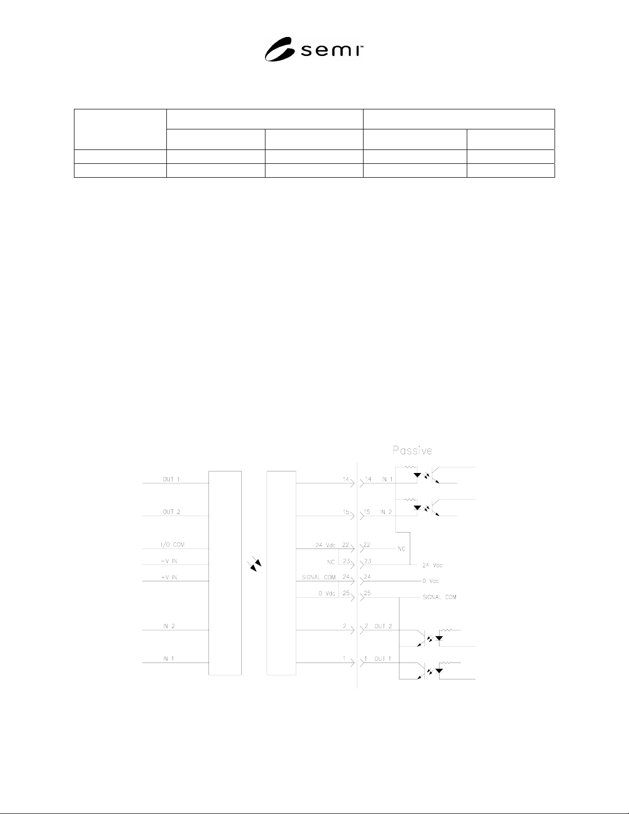
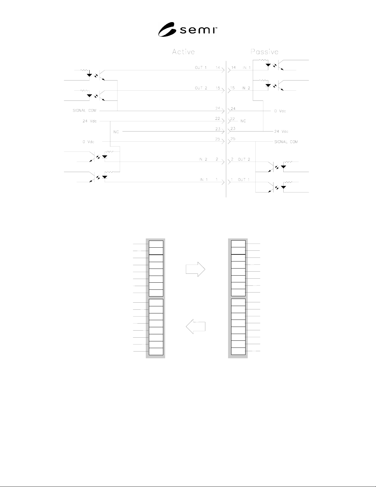
6.4.5 All configurations will include signal optoisolation within each equipment conforming to this standard to
allow for optical transmission or hardwired configuration to coexist. See Figures 32 and 33 below.
6.4.6
Timing diagram signal state of Off corresponds to no current flow for the hardwired configuration or no
optical signal transmitted for the optical transmitter configurations.
6.5
Interface Sensor Unit Size
6.5.1 The maximum dimensions in millimeters of the interface sensor are indicated in Figure 37. This size includes
volume needed for rigid portions of the sensor’s electrical connector and cable. For systems which are designed to
handle 300 mm wafer carriers, the interface sensor unit must be designed in a way that allows mounting of the unit
within the exclusion volume as defined per SEMI E15.1 with the optical axis centered in this exclusion volume.
A
ct i ve
Figure 32
Optoisolated Implementation Using an Optical Transmission Device
SEMI E84-0305 © SEMI 1999, 2005 31
Figure 33
Optoisolated Implementation Using Hardwired Connection
Input
Output
Output
Input
VA L I D
CS_0
CS_1
AM_AVBL*
TR_REQ
BUSY
COMPT
CONT
L_REQ
U_REQ
VA *
READY
VS_0*
VS_1*
HO_AVBL
ES
3
4
5
1
2
6
7
8
2
3
4
5
6
7
8
1
3
4
5
3
4
5
1
2
6
7
8
2
3
4
5
6
7
8
1
3
4
5
VA L I D
CS_0
CS_1
TR_REQ
BUSY
COMPT
CONT
L_REQ
U_REQ
READY
HO_AVBL
ES
Active Passive
AM_AVBL*
VA *
VS_0*
VS_1*
* This signal is for interbay passive OHS vehicle use only.
Figure 34
Bit Assignments for Interlock Signal between Passive and Active

SEMI E84-0305 © SEMI 1999, 2005 32
12
141516
345678910111213
171819202122232425
OUT1
OUT2
OUT3
OUT4
OUT5
OUT6
OUT7
OUT8
NC (See NOTE 1)
Reserved (See NOTE 2)
Reserved (See NOTE 2)
Reserved (See NOTE 2)
NC (See NOTE 1)
Signal COM
Power COM
Power
NC (See NOTE 1)
IN8
IN7
IN6
IN5
IN4
IN3
IN2
IN1
NOTE 1: NC = Not Connected
NOTE 2: Reserved = The pin may be used to support the signal required for a type of any interface unit. It cannot be used for
current or future implementations of this specification.
Figure 35
Pin Assignments for Connector of Passive Equipment Side (Pin Side View)
12
14 15 16
345678910111213
17 18 19 20 21 22 23 24 25
OUT8
OUT7
OUT6
OUT5
OUT4
OUT3
OUT2
OUT1
NC (See NOTE 1)
Reserved (See NOTE 2)
Power COM
Signal COM
Power
IN1
IN2
IN3
IN4
IN5
IN6
IN7
IN8
Reserved (See NOTE 2)
Reserved (See NOTE 2)
NC (See NOTE 1)
NC (See NOTE 1)
Figure 36
Pin Assignments for Connector of Active Equipment Side (Pin Side View)