semi合集-English.pdf - 第7383页
SEMI MF1451-1104 © SEMI 2004 7 RELATED INFORMATION 1 MEASUREMENT ERRORS DUE TO DIFFERENCES IN DIAMETER AND THICKNESS BETWEEN A REPRESEN TATIVE WAFER AND A WAFER UNDER TEST NOTICE: This related information is no t an offi…
SEMI MF1451-1104 © SEMI 2004 6
13.15.1 Record sample standard deviation and other
statistical parameters as agreed upon between the
parties to the test.
14 Report
14.1 Report the following information:
14.1.1 Date, time, and temperature of test,
14.1.2 Identification of operator,
14.1.3 Location (laboratory) of test,
14.1.4 Identification of measuring instruments,
including wafer-holding device diameter, data point
spacing, sensor size, and gravitation-correction method,
14.1.5 Lot identification, including nominal diameter,
nominal center-point thickness, and nominal edge
exclusion (EE) specified.
14.1.6 Description of sampling plan, if any, and
14.1.7 Sori of each wafer measured.
14.2 For referee tests also include in the report the
standard deviation of each set of wafer measurements
and such other statistical parameters as have been
agreed to by the parties to the test.
15 Precision
15.1 An inter-laboratory experiment to establish the
precision of this test method has not been conducted.
15.2 In order to estimate the precision, an error analysis
was performed in accordance with ASTM Practice D
4356. This analysis indicates the best 1s precision
obtainable by this method is ±0.35 m.
15.3 This value is obtained as follows:
15.3.1 The instrument resolution is specified to be 0.1
m. Therefore, the values a and b cannot be known
closer than this during each of the six measurements
made during the determination of sori:
two measurements on the reference wafer in the
normal orientation,
two measurements on the reference wafer in the
inverted orientation, and
two measurements on the sample wafer in the
normal orientation.
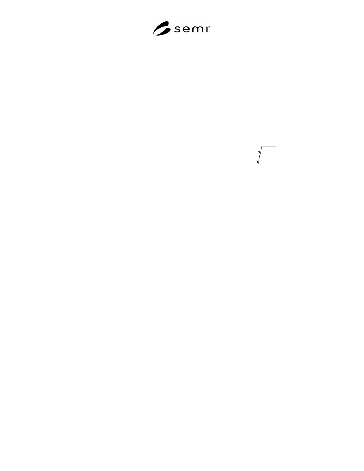
15.4 Equation A1.1 in ASTM Practice D 4356 holds
that:
35.0
6)1.0(2
2e (1s)Precision
2
2
N
(14)
where:
e =
single measurement error (0.1 m), and
N = number of measurements made during the
determination of sori (6).
15.5 In practice, this precision is degraded by the
factors listed in Section 3.
16 Bias
16.1 Bias — No standards exist against which the bias
of this test method can be evaluated.
17 Keywords
non-contact measurement; semiconductor; shape;
silicon; sori; wafers
SEMI MF1451-1104 © SEMI 2004 7
RELATED INFORMATION 1
MEASUREMENT ERRORS DUE TO DIFFERENCES IN DIAMETER AND
THICKNESS BETWEEN A REPRESENTATIVE WAFER AND A WAFER
UNDER TEST
NOTICE: This related information is not an official part of SEMI MF1451. This related information was approved
for publication by full letter ballot on August 16, 2004.
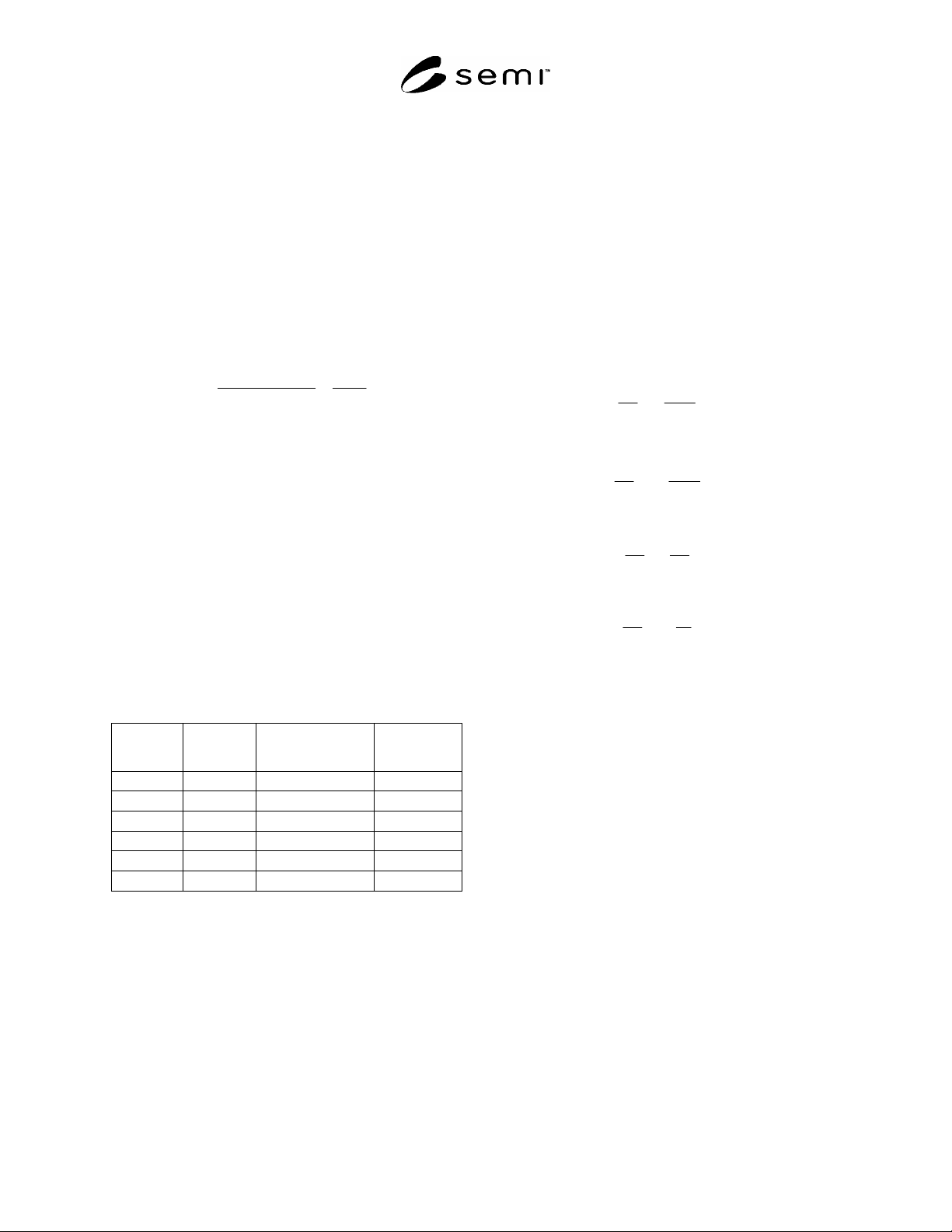
R1-1 The sag, or deflection induced by gravity at the
edge of a wafer supported at its center, in m, has been
estimated
3
as:
2
4
2
48
32
)103(
t
KD
Et
kgdD
S
(R1-1)
where:
S =
deflection , in m,
k = geometrical constant (=0.5854),
g = gravitational constant (980 cm/s
2
),
d = density of silicon (2.329 g/cm
3
),
E =
Young’s modulus (~1.610
12
dyne/cm
2
,
D = nominal wafer diameter, in mm, and
t =
nominal wafer thickness, in m.
K, the constant of proportionality is therefore equal to
7.83 10
3
m
3
/mm
4
. Table R1-1 gives estimated
values of sag in micrometers for 100 mm through 300
mm diameter wafers with thickness and diameter as
specified in SEMI M1.
Table R1-1. Estimated Sag, in
m, of Wafers of
Nominal Diameter and Thickness
Diameter,
mm
Thickness,
m
SEMI M1 Reference Estimated Sag,
m
300 775 SEMI M1.15 105.6
200 725 SEMI M1.9 23.8
150 675 SEMI M1.8 8.7
150 625 SEMI M1.13 10.1
125 625 SEMI M1.7 4.9
100 525 SEMI M1.5 2.8
R1-2 For small variations about the nominal values of
diameter and thickness, the relative change of the
gravity effect is 4 times the relative change of the
diameter and 2 times the relative change of thickness:
2
3
4
t
Kd
d
S
(R1-2)
and
3
4
2
t
Kd
t
S
(R1-3)
Therefore the relative changes are as follows:
d
d
S
S
4 (R1-4)
and
t
t
S
S
2 (R1-5)
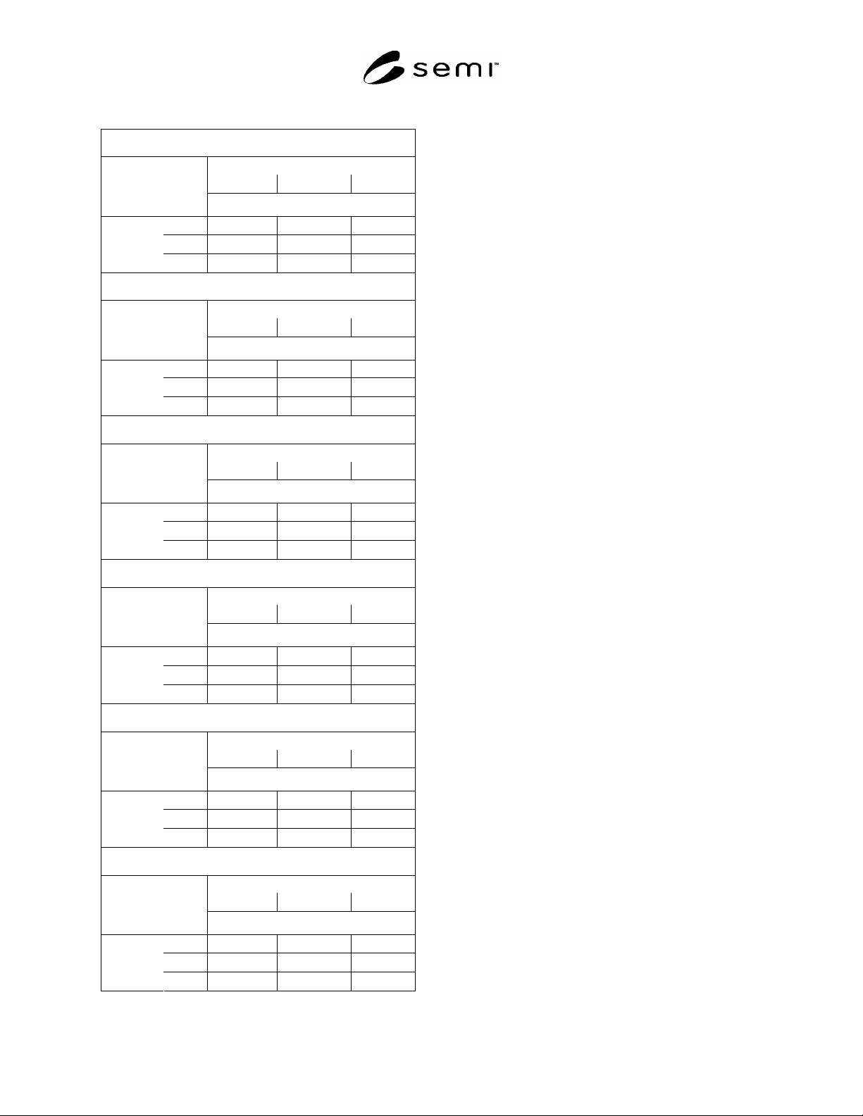
R1-3 Table R1-2 gives examples of worst-case gravity
effect errors (in micrometers), for 100 mm through 300
mm diameter wafers with thickness and diameter toler-
ances as specified in SEMI M1.
SEMI MF1451-0704 © SEMI 2004 8
Table R1-2 Examples of Gravity Effect Errors
NOTICE: SEMI makes no warranties or
representations as to the suitability of the standards set
forth herein for any particular application. The
determination of the suitability of the standard is solely
the responsibility of the user. Users are cautioned to
refer to manufacturer's instructions, product labels,
product data sheets, and other relevant literature,
respecting any materials or equipment mentioned
herein. These standards are subject to change without
notice.
By publication of this standard, Semiconductor
Equipment and Materials International (SEMI) takes no
position respecting the validity of any patent rights or
copyrights asserted in connection with any items
mentioned in this standard. Users of this standard are
expressly advised that determination of any such patent
rights or copyrights, and the risk of infringement of
such rights are entirely their own responsibility.
300 mm Diameter Wafers
Actual Diameter, mm
299.8 300.0 300.2
Gravity Effect Errors,
m
755 3.90 5.67 5.96
775
1.68
0.00 0.28
Actual
Thickness,
m
795
6.84 5.25 4.98
200 mm Diameter Wafers
Actual Diameter, mm
199.8 300.0 200.2
Gravity Effect Errors,
m
705 0.77 1.37 1.47
725
0.57
0.00 0.10
Actual
Thickness,
m
745
0.52 1.26 1.17
150 mm Diameter Wafers
Actual Diameter, mm
149.8 150.0 150.2
Gravity Effect Errors,
m
655 0.49 0.54 0.59
675
0.05
0.00 0.05
Actual
Thickness,
m
695
0.54 0.49 0.45
150 mm Diameter Wafers
Actual Diameter, mm
149.8 150.0 150.2
Gravity Effect Errors,
m
610
0.45
0.51 0.56
625
0.05
0.00 0.05
Actual
Thickness,
m
640
0.52 0.47 0.42
125 mm Diameter Wafers
Actual Diameter, mm
124.5 125.0 125.5
Gravity Effect Errors,
m
605 0.25 0.33 0.41
625
0.08
0.00 0.08
Actual
Thickness,
m
645
0.37 0.30 0.22
100 mm Diameter Wafers
Actual Diameter, mm
99.5 100.0 100.5
Gravity Effect Errors,
m
505 0.17 0.23 0.29
525
0.06
0.00 0.06
Actual
Thickness,
m
545
0.26 0.20 0.15
Copyright by SEMI® (Semiconductor Equipment and Materials
International), 3081 Zanker Road, San Jose, CA 95134. Reproduction of
the contents in whole or in part is forbidden without express written
consent of SEMI.