semi合集-English.pdf - 第163页
SEMI E21-94 © SEMI 1991, 2002 3 provided in the O-ring flange face as shown in Figure 1 and specified i n Figure 3. Alignm ent pin height above the flange fac e is 6 mm (0.24 in. ) minim um to 8 mm (0.31 in.) m aximum (s…

SEMI E21-94 © SEMI 1991, 2002 2
5.1.9 process module — a module that accepts or
presents a single wafer inside the module for intratool
transport.
5.1.10 reach — the distance measured from the
interface plane to the wafer centroid within a process or
cassette module.
5.1.11 transport module — a module that accepts or
presents a single wafer outside the module across the
interface plane for intratool transport.
5.1.12 wafer transport plane — the horizontal surface
a wafer traverses between modules.
5.1.13 wafer transport zone — the area of the interface
plane free of physical obstructions, reserved for wafer
movement between modules.
6 Requirements
6.1 Wafer Transport and Placement
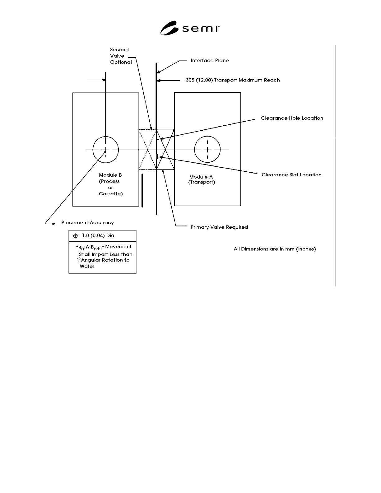
6.1.1 Horizontal Transport Plane — The dimensions
for wafer placement during wafer transport are
referenced from the interface plane in the plan view
shown in Figure 1. The transport module is required to
present or accept a horizontal wafer outside the module
anywhere along an axis perpendicular to the center of
the interface plane to a maximum 305 mm (12 in.) from
the interface plane. Thus, a transport module is required
to have the capability to reach 305 mm (12 in.) beyond
its interface plane to a wafer centroid (see Section R1-
1). However, location of the wafer at a distance less
than 305 mm (12 in.) from the interface plane requires
that the transport module be capable of addressing the
intermediate location. Similarly, a cassette module or
process module accepts a horizontal wafer inside the
module anywhere along an axis perpendicular to the
center of its interface plane up to a maximum 305 mm
(12 in.) from the interface plane as required by the
application.
6.1.1.1 Placement Accuracy — The requirements for
placement accuracy of a wafer in the horizontal plane
within a module are 1.0 mm (0.04 in.) true position, ±
0.5 mm (± 0.020 in.) radially, with less than one degree
angular rotation for every module-to-transport-to-
module wafer transport (B
n
:A:B
n
+ 1as shown in Figure
1). If the wafer is displaced in the process module, it
must be returned to the original position within the non-
culmulative placement accuracy of 1.0 mm (0.04 in.)
true position, ± 0.5 mm (± 0.020 in.) radially.
6.1.2 Vertical Position of Transport Plane — The
elevation of the wafer transport plane is measured from
the facility floor as shown in Figure 2. The transport
module is required to present or accept a horizontal
wafer outside the module at a nominal wafer transport
height of 1100 mm (43.307 in.) from the facility floor
(see Section R1-2).
6.1.2.1 Vertical Motion — The transport module is
required to move the wafer to within ± 0.5 mm (0.020
in.) in the wafer transport plane. The transport module
is also required to posess a vertical motion capability to
a second plane 6.0 mm ± 0.5 mm (0.236 in. ± 0.020 in.)
below the wafer transport plane in order to allow wafer
handoff to or from passive cassette or process modules
(see Figure 2 and Section R1-3).
6.1.2.2 Reference Plane — The interface plane
alignment pins define a reference plane 9.5 mm (0.374
in.) below the wafer transport plane (see Figure 2).
6.2 Interface Plane — The interface plane contains the
interface seal zone and the wafer transport zone, which
do not overlap, and the location of the interface plane
alignment pins (see Figures 3 and 4).
6.2.1 Interface Seal Zone — The interface seal zone is
rectangular and symmetrically referenced to the
interface plane alignment pins. The inside boundary
dimension of the interface seal zone is 46 mm (1.811
in.) by 236 mm (9.291 in.). The outside boundary is 76
mm (2.992 in.) by 266 mm (10.472 in.). A seal zone is
either a seal surface or an O-ring face. All interface seal
zones facing toward a transport module are seal
surfaces polished to a surface finish less than or equal to
0.8 micrometer (32 microinches) parallel to the
circumference (see Section R1-4). All interface seal
zones facing toward a cassette or process module are O-
ring faces equipped with the appropriate capture groove
for the sealing method employed (see Figure 3 and
Section R1-4.1).
6.2.2 Wafer Transport Zone — The wafer transport
zone is the area within the interface seal zone reserved
for moving the wafer between modules. The wafer
transport zone which cannot be compromised by any
module is defined as the area at least 16 mm (0.630 in.)
above and below the alignment pin centerlines, and 111
mm (4.370 in.) to the left and right of the centerline
between the two alignment pins (see Figure 3 and
Section R1-5).
6.2.3 Interface Plane Alignment Pins — Provisions are
made for two 10 mm (0.394 in.) diameter locating pins
(see Figure 4) to be used as alignment aids between
modules. Under no circumstances should the flanges at
the interface plane and the alignment pins be subject to
a total load exceeding 500N (112 lbf) in shear. The
alignment pins have an absolute centerline separation of
300.0 mm (11.811 in.) in the horizontal plane. The pins
reside in the seal surface side of the flange pair,
opposite the O-ring, facing toward the transport
module. Mild press fit holes are provided in the seal
surface flange face. A clearance hole and a slot are

SEMI E21-94 © SEMI 1991, 2002 3
provided in the O-ring flange face as shown in Figure 1
and specified in Figure 3. Alignment pin height above
the flange face is 6 mm (0.24 in.) minimum to 8 mm
(0.31 in.) maximum (see Section R1-6).
6.2.4 Isolation Valves — The transport module is
always equipped with a valve for environmental
isolation at each module interface plane. The intratool
transport port on a process or cassette module may be
equipped with an environmental isolation valve (see
Section R1-7).
6.3 Flange — A flange is specified as 162 mm (6.378
in.) by 340 mm (13.386 in.). One horizontal edge is
specified to be 50 mm (1.969 in.) from the alignment
pins’ centerline (see Figure 4).
6.3.1 Clamping — Clamping grooves as specified in
the International Standards Organization document,
Vacuum Technology, Flange Dimensions (ISO 1609-
1986), Table 2, nominal bores 40 mm-250 mm (1.575
in.Ð9.843 in.) are located at the flange perimeter (see
groove detail in Figure 4). Clamps for ISO flanges can
be used to generate the force necessary to produce an
environmental seal (see Section R1-8).
6.3.2 Non-Flanged Surfaces — A non-flanged surface
may be used to join with a flanged surface. An
attachment means to engage the flange must be
provided. If a flanged adaptor piece is necessary to join
two non-flanged surfaces, then the adaptor piece shall
be located on the process or cassette side of the
interface plane.
LIST OF FIGURES
Figure 1 — Module Interface with Wafer Transport and
Placement Detail (Plan View)
Figure 2 — Wafer Transport Plane Elevation
Figure 3 — Interface Plane
Figure 4 — Flange Specification
SEMI E21-94 © SEMI 1991, 2002 4
Figure 1
Module Interface with Wafer Transport and Placement Detail (Plan View)