semi合集-English.pdf - 第7646页
SEMI T5-96 © SEMI 1996, 2004 9
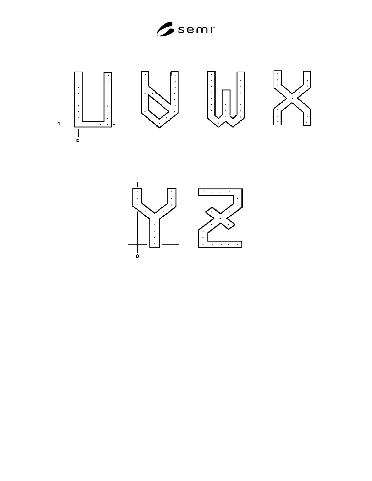
SEMI T5-96 © SEMI 1996, 2004 8
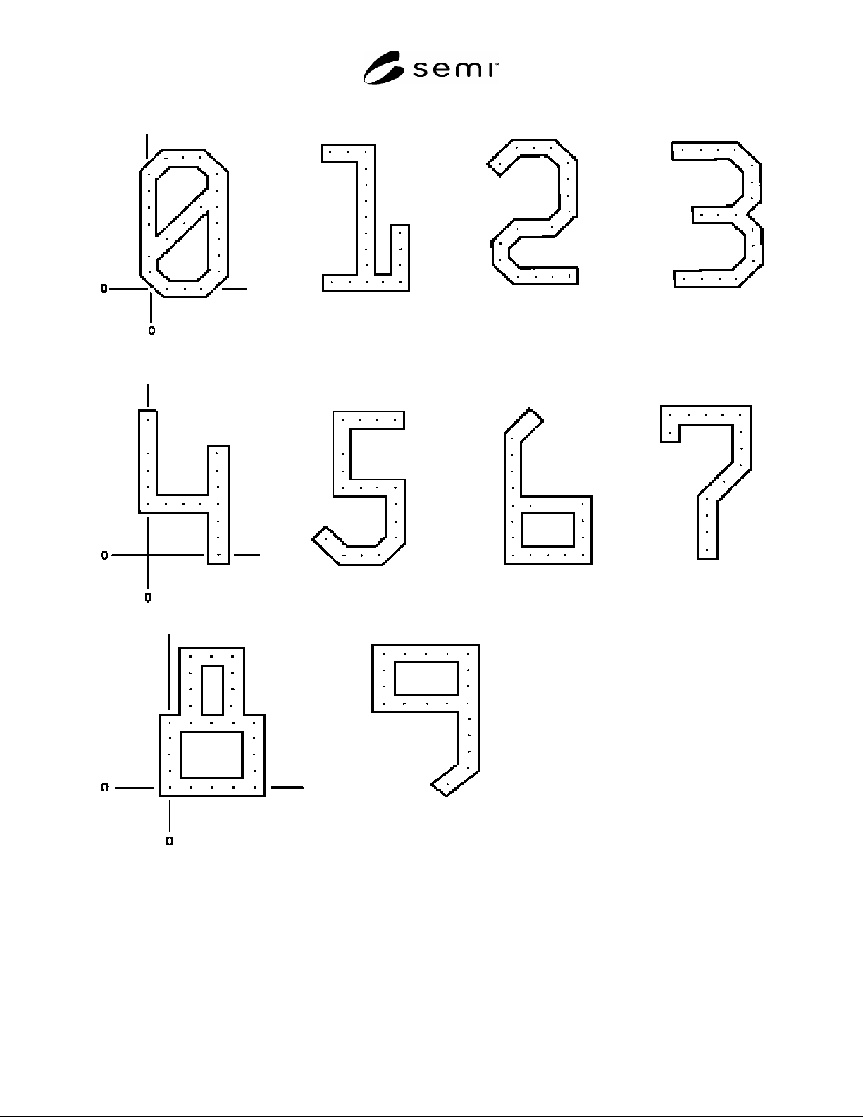
SEMI T5-96 © SEMI 1996, 2004 9

SEMI T5-96 © SEMI 1996, 2004 10
RELATED INFORMATION 1
NOTICE: This related information is not an official part of SEMI T5. This related information was approved for
publication by full letter ballot procedures.
R1-1 Considerations for Reliable Automatic
Reading of the Marking
R1-1.1 The following suggestions are offered to assist
in assuring the most reliable automatic reading of the
alphanumeric marking.
R1-1.2 Character Stroke Thickness — If a 5 × 9 dot
matrix is chosen for marking, it is recommended that
the minimum dot size be 0.100 mm. Double or higher
density dot matrix is recommended; when used, smaller
dot diameters may be employed. Stroke thickness
should be constant withing 20% over the entire
character set so that the reader settings may be
optimized for the specific wafer run.
R1-1.3 Contrast — The character should have
sufficient contrast to be legible. Contrast may be
affected by depth and other conditions.
R1-1.4 Clear Zone — It is recommended that the area
immediately beneath and a minimum of 0.500 mm
around the marking characters be of uniform
reflectivity and free of any lithography and process
overlay edges.
R1-2 Considerations for the Use of Front
Surface Markings
R1-2.1 Marks can impinge upon areas where devices
may be printed. Since mask geometries are varied,
considerations of the mark area should be made in mask
design and also when applying the mark specifications
to existing mask designs.
R1-2.2 When the mark is applied prior to epitaxial
deposition, a crown or epi may grow along the mark
edge. The height of this crown will depend upon the epi
thickness and the deposition process.
NOTICE: SEMI makes no warranties or
representations as to the suitability of the standards set
forth herein for any particular application. The
determination of the suitability of the standard is solely
the responsibility of the user. Users are cautioned to
refer to manufacturer's instructions, product labels,
product data sheets, and other relevant literature,
respecting any materials or equipment mentioned
herein. These standards are subject to change without
notice.
By publication of this standard, Semiconductor
Equipment and Materials International (SEMI) takes no
position respecting the validity of any patent rights or
copyrights asserted in connection with any items
mentioned in this standard. Users of this standard are
expressly advised that determination of any such patent
rights or copyrights, and the risk of infringement of
such rights are entirely their own responsibility.
Copyright by SEMI® (Semiconductor Equipment and Materials
International), 3081 Zanker Road, San Jose, CA 95134. Reproduction of
the contents in whole or in part is forbidden without express written
consent of SEMI.