semi合集-English.pdf - 第5360页
SEMI M54-0304 © SEMI 2003, 2004 1 SEMI M54-0304 GUIDE FOR SEMI-INSULATING (SI) GaAs MATERIAL PARAMETERS This guide was technically approved by the Global Com pound Semiconductor Committee and is the direct responsibility…
SEMI M53-1103 © SEMI 2003 10
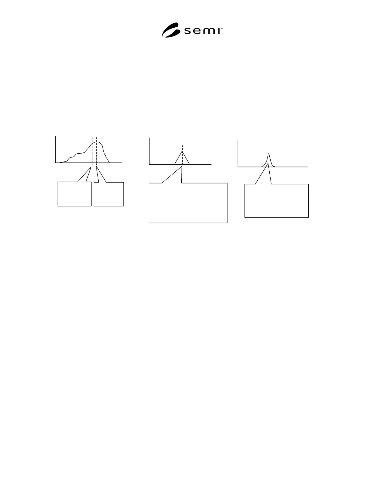
R1-1.5 The accuracy of the peak diameter, which is specified to have a relative expanded uncertainty at about 95%
confidence level as small as possible but not greater than 3% in SEMI M52, is determined by either the accuracy
with which the peak source diameter is known (or can be found), or by the accuracy of the DMA sweep
voltage/diameter relationship. Unfortunately many PSL source bottles currently in use do not give the peak
diameter, so this presents a difficulty for the first approach. The second approach, relying on DMA voltage
accuracy, can be checked by using PSL sources that are known to be very narrow (to minimize differences between
source and deposition peak diameter) with very accurate peak values.
PSL Source Diameter
Distribution
Mean, or
average,
diameter
Peak, or
modal,
diamete
Diameter
Counts/Diameter
X =
Deposition Transfer
Function
In many deposition
systems, the transfer
function may be scanned
through the diameter
distribution and set to the
p
eak diameter.
Transmission
Diameter
Deposition Diameter
Distribution
Diameter
Counts/Diameter
The shape of the
deposition diameter
distribution is no
wider than the
transfer function.
Figure R1-1
The Diameter Distribution of the Deposition is the Product of the Deposition System Transfer Function and
the Source (or “Bottle”) Distribution.
NOTICE: SEMI makes no warranties or representations as to the suitability of the standards set forth herein for any
particular application. The determination of the suitability of the standard is solely the responsibility of the user.
Users are cautioned to refer to manufacturer's instructions, product labels, product data sheets, and other relevant
literature, respecting any materials or equipment mentioned herein. These standards are subject to change without
notice.
By publication of this standard, Semiconductor Equipment and Materials International (SEMI) takes no position
respecting the validity of any patent rights or copyrights asserted in connection with any items mentioned in this
standard. Users of this standard are expressly advised that determination of any such patent rights or copyrights, and
the risk of infringement of such rights are entirely their own responsibility.
Copyright by SEMI® (Semiconductor Equipment and Materials
International), 3081 Zanker Road, San Jose, CA 95134. Reproduction o
f
the contents in whole or in part is forbidden without express written
consent of SEMI.

SEMI M54-0304 © SEMI 2003, 2004 1
SEMI M54-0304
GUIDE FOR SEMI-INSULATING (SI) GaAs MATERIAL PARAMETERS
This guide was technically approved by the Global Compound Semiconductor Committee and is the direct
responsibility of the European Compound Semiconductor Materials Committee. Current edition approved by
the European Regional Standards Committee on January 9, 2004. Initially available at www.semi.org
February 2004; to be published March 2004. Originally published March 2003.
1 Purpose
1.1 Substrates with high electrical resistivity and
electron drift mobility are needed to fabricate high
performance digital and analog microelectronic devices
and circuits. Semi-insulating n-type Gallium Arsenide,
henceforth termed SI GaAs, has been established
worldwide as a preferred substrate material for such
applications.
1.2 The active layers needed for devices are generated
either by ion implantation or by epitaxy. The quality of
these layers, and hence the performance, yield and
reliability of devices, strongly depends on the bulk and
surface quality of the substrate.
1.3 This document provides a basis for specifying the
material parameters of SI GaAs to support ordering
agreements between suppliers and purchasers.
2 Scope
2.1 This document defines and describes the electrical,
optical, structural, and surface properties of SI GaAs
that are considered technically relevant according to the
present status of scientific knowledge and material
technology.
2.2 A specification of the material quality of SI GaAs
substrates includes a number of the parameters
described below. Depending on the intended
application, a particular subset of properties and
respective parameters will be considered relevant by the
purchaser.
2.3 In order to enhance the clarity and applicability of
the document, the ordering information in Section 6
subdivides the material parameters in respect of their
relative importance, according to general industry
perception.
2.4 Some material properties and parameters, while
intensively discussed in the technical literature, are
insufficiently established to allow an unambiguous
specification. The available information is nevertheless
included to support supplier-purchaser discussions and
agreements on these issues.
2.5 Each parameter specification requires an agreement
about verification. Appropriate information is
summarized in Section 5. Available standard test
methods elaborated by SEMI, ASTM, and DIN are
referenced in Section 3.
2.6 A number of the required standard test methods do
not exist at present. This document is expected to serve
as a guideline and incentive for qualified ASTM, DIN,
JEITA, and SEMI committees to develop the missing
standard procedures. Conversely, if at present more
than one standard test method for verification of a
specific parameter exists (see Table 1), a global
consensus procedure towards selecting or generating a
unique standard is advocated.
2.7 The geometrical properties of wafers, in particular
orientation, diameter, thickness, flatness and edge
rounding, are covered by the series of SEMI M9
specifications and shall not be addressed here.
NOTICE: This standard does not purport to address
safety issues, if any, associated with its use. It is the
responsibility of the users of this standard to establish
appropriate safety and health practices and determine
the applicability of regulatory or other limitations prior
to use.
3 Referenced Standards
3.1 SEMI Standards
SEMI M9 — Specifications for Polished
Monocrystalline Gallium Arsenide Slices
SEMI M10 — Standard Nomenclature for
Identification of Structures and Features Seen on
Gallium Arsenide
SEMI M15 — Polished Wafer Defect Limits Table for
Polished Gallium Arsenide Wafers
SEMI M30 — Standard Test Method for Substitutional
Atomic Carbon Concentration in GaAs by Fourier
Transform Infrared Absorption
SEMI M36 — Test Method for Measuring Etch Pit
Density (EPD) in Low Dislocation Density Gallium
Arsenide Wafers
SEMI M39 — Test Method for Measuring Resistivity
and Hall Coefficient and Determining Hall Mobility in
Semi-insulating GaAs Single Crystals

SEMI M54-0304 © SEMI 2003, 2004 2
3.2 ASTM Standards
1
ASTM F76 — Standard Test Methods for Measuring
Resistivity and Hall Coefficient and Determining Hall
Mobility in Single-Crystal Semiconductors
ASTM F1404 — Test Method for Crystallographic
Perfection of Gallium Arsenide by Molten Potassium
Hydroxide (KOH) Etch Technique
3.3 DIN Standards
2
DIN 50448 — Testing of materials for semiconductor
technology - Contactless determination of the electrical
resistivity of semi-insulation semiconductor slices using
a capacitive probe
DIN 50449-1 — Testing of materials for semiconductor
technology - Determination of impurity content in
semiconductors by infrared absorption - Part 1: Carbon
in gallium arsenide
DIN 50449-2 — Testing of materials for semiconductor
technology - Determination of impurity content in
semiconductors by infrared absorption - Part 2: Boron
in gallium arsenide
DIN 50454-1 — Testing of materials for semiconductor
technology - Determination of dislocations in
monocrystals of III-V-compound semiconductors - Part
1: Gallium arsenide
NOTICE: Unless otherwise indicated, all documents
cited shall be the latest published versions.
4 SI GaAs
4.1 SI GaAs as described in this specification has n-
type conductivity and an electrical resistivity ρ in the
range 1 × 10
6
– 5 × 10
8
Ωcm. It is characterized by
fabrication procedures and material properties.
4.2 Synthesis of the compound GaAs from the
elements gallium (Ga) and arsenic (As) may be done
• in the crystal growth chamber immediately prior to
growth (in-situ synthesis)
• in separate equipment, independent of crystal
growth (ex-situ synthesis)
4.3 The growth of SI GaAs single crystals involves one
of the following procedures:
• Liquid Encapsulated Czochralski (LEC)
1 Available from American Society for Testing and Materials, 100
Barr Harbor Drive, West Conshohocken, Pennsylvania 19428-2959,
USA. Telephone: 610.832.9585, Fax: 610.832.9555 Website:
www.astm.org
2 Available from Deutches Institut für Normung e.V., Beuth Verlag
GmbH, Burggrafenstrasse 4-10, D-10787 Berlin, Germany, website:
www.din.de
• LEC with controlled As vapor pressure (VCZ)
• Vertical Gradient Freeze (VGF)
• Vertical Bridgman (VB)
4.4 SI GaAs single crystal ingots are thermally treated
after crystal growth. The annealing procedures are
defined by heating rates, hold temperatures, hold times
and cooling rates. Single step ingot annealing (one hold
time at one temperature) or multi step ingot annealing
(several hold times at different temperatures) may be
applied. Wafers may be treated similarly by single step
wafer annealing and multi step wafer annealing.
4.5 SI GaAs contains the intrinsic double donor point
defect EL2, which involves an As atom on a Ga site
(As
Ga
). At room temperature the first ionization level
EL2
0
/EL2
+
is approximately at ∆E = 0.69 eV below the
conduction band. The concentration [EL2
0
] of the neu-
tral defect is in the range of 5 × 10
15
to 3 × 10
16
cm
-3
.
4.6 SI GaAs contains unintentionally incorporated
impurities acting as donors. It may also contain
intrinsic donor defects other than EL2. The total
concentration [D] of donors other than EL2 should be
low for optimal control of ion implantation activation
and high electron mobility µ (see Section 4.12).
4.7 SI GaAs contains impurities acting as acceptors. It
may also contain intrinsic acceptor defects. Usually the
total concentration [A] of acceptors is adjusted by
controlled incorporation of carbon (C) in the
concentration range [C] 4 × 10
14
cm
-3
– 2 × 10
16
cm
-3
.
4.8 SI GaAs contains extrinsic and intrinsic point
defects that do not participate in the compensation
process (see Sections 4.10 and 4.11). These defects
may be isoelectronic centers (e.g. boron (B)
incorporated on the Ga site, B
Ga
) or extremely deep
donors and acceptors below and above the Fermi level,
respectively. They may influence the material quality,
for instance by degrading the activation efficiency of
implanted dopants or by acting as transient carrier traps
and nonradiative recombination centers (NRRC).
4.9 SI GaAs generally is nonstoichometric, containing
excess As with a concentration of the order of
10
18
cm
-3
. The excess As is partly incorporated as
lattice antisite defects (As
Ga
), see Section 4.5. Other
forms of point defect incorporation (e.g. interstitial As)
are likely, but have not been positively identified.
Excess As is attracted by dislocations (see Section 4.13)
and is concentrated along these, forming decoration
precipitates. Precipitates may also be generated away
from dislocations, e.g. in the inner part of dislocation
cells (see Section 4.14). They are referred to as matrix
precipitates and are generally smaller than dislocation
precipitates. The concentration and size of precipitates