semi合集-English.pdf - 第4246页
SEMI F77-0703 © SEMI 2003 5 APPENDIX 1 EXAMPLE OF A CPT TEST PROC EDURE NOTICE : The material in this appendix is an official pa rt of SEM I F77 and was approved by full letter ball ot procedures. A1-1 Principle A1-1.1 C…

SEMI F77-0703 © SEMI 2003 4
Alternately, plater’s tape can also be used, leaving 0.25
in. uncovered at the end for electrical contact.
9.4 Finish — In general, refer to ASTM G150 for
details on the typical finish of the test specimens. Since
surface finish can effect the CPT results, surface
finished should be done as consistently as possible
within a sample set. Details of the surface finishing
process, parameters and characterization should be
provided in the test report as outlined in Section 15.
9.5 Sampling — It is recommended that a minimum of
3 specimens, and preferably 5 or more, should be used
to obtain statistical significance in the testing results.
9.6 Test Area — In general, refer to ASTM G150,
which states a minimum test area of 1 cm
2
. This
minimum test area is required for both flat specimens
and tubing specimens.
10 Reagents And Materials
10.1 In general, refer to Section 8 of ASTM G150
describing the purity of the reagents and water needed
for the test solution as well as the purity of the N
2
purging gas.
10.2 Standard Test Solution — Comparison of the CPT
results requires consistency in the test solution, so it is
recommended that a 1 M (mole/liter) sodium chloride
(NaCl) electrolyte be used as electrolyte. However,
because of the different processes gases used by the
semiconductor industry (HCl, HBr, Cl
2
, BCl
3
, HF,
WF
6
), it is possible to substitute another test solution to
represent the particular anion of the process gas which
may impart different pitting characteristics (e.g., 1 M
NaBr, or 1M NaF).
11 Applied Potential
11.1 Stainless Steel — In general, refer to section 9 of
ASTM G150, which provides the standard anodic
potential commonly used for most stainless steels (an
anodic potential of 700 mV versus SCE at 25°C).
Section 9 also provides an alternative potential if there
is uncertainty as to whether this potential is sufficiently
high to obtain a potential independent CPT.
11.2 Alternative Alloys — Alloys other than 316L
stainless steel can be tested using the applied potential
given in Section 11.1.
12 Procedure
12.1 In general refer to Section 10 of ASTM G150 for
details on specimen mounting, cleaning, and placement,
test solution preparation, test procedure, and completion
of the test.
12.2 Refer to Annexes A1 and A2 in ASTM G150 for
guidelines to calibrate the specimen temperature.
12.3 Tubing specimens — Tubing testing requires
different specimen mounting and preparation than given
in Section 9 of ASTM G150. Tubing specimens should
be placed vertically in solution so that approximately
one inch is submerged.
13 Visual Examination Of Test Specimen
13.1 In general, refer to Section 11 of ASTM G150 for
a description of the visual examination of the test
specimen.
14 Data Analysis
14.1 In general, refer to Section 12 of ASTM G150 for
details on evaluating the critical pitting temperature.
15 Reporting Results
15.1 Section 13 of ASTM G150 provides a list of
mandatory information required in the test report.
15.2 Other mandatory information that should be
provided are the starting test electrolyte composition,
the diameter of the tubing for tubing specimens,
identification of the surface finish process (e.g.,
electropolish, passivation), and any other specific
parameters or characterization related to the surface
finish process. Welded and non-welded specimens
should also be clearly identified, as well the welding
procedure used to weld the specimen.
16 Precision and Bias
16.1 The precision of this test method is yet to be
determined
16.2 The bias of this test method is yet to be
determined.
17 References
17.1 Blum, Michael. M.S. Thesis. University of
London, England, December 1970.
17.2 Philip A. Schweitzer, Ed. “Corrosion and
Corrosion Protection Handbook.” Marcel Dekker, New
York, p. 11, 1983.

SEMI F77-0703 © SEMI 2003 5
APPENDIX 1
EXAMPLE OF A CPT TEST PROCEDURE
NOTICE: The material in this appendix is an official part of SEMI F77 and was approved by full letter ballot
procedures.
A1-1 Principle
A1-1.1 Critical pitting temperature (CPT) is an
electrochemical test that determines the localized
corrosion resistance of stainless steel and other alloys.
The test is performed in a solution of sodium chloride
(NaCl). The sample is polarized at 700 mV
SCE
while
the temperature is gradually increased from 0°C at a
rate of 1°C/min. Above some critical temperature,
pitting corrosion will occur signified by a rapid increase
in measured current above 100 µ A/cm
2
for 60 seconds.
The experiment is monitored and controlled using
special software.
A1-2 Precautions
A1-2.1 Use caution with heating mantles, as they can
become very hot.
A1-3 Equipment and Supplies
A1-3.1 Corrosion Test System (potentiostat and
software)
A1-3.2 Chiller (capable of –10°C to 100° C)
A1-3.3 Temperature controller
A1-3.4 Heating Mantle
A1-3.5 Stir Plate/Bar (Immersible)
A1-3.6 Glass cell (adapted to contain electrodes,
probes, and cooling coil)
A1-3.7 Counter electrodes (graphite rods)
A1-3.8 Reference electrode (saturated calomel) and
luggin probe
A1-3.9 Cooling coils
A1-4 Chemicals and Reagents
A1-4.1 Sodium Chloride (ACS Reagent Grade)
A1-4.2 18 MΩ deionized water
A1-5 Procedure
A1-5.1 Turn chiller on and set at -2°C.
A1-5.2 Fill Beaker with 800 ml of 1 M (mole/liter)
NaCl electrolyte (Preferably chilled in refrigerator).
Turn stir plate on and ensure adequate stirring with stir
bar.
A1-5.3 Turn on temperature controllers. Adjust set
point to –1°C. Place lid on beaker and ensure
temperature probe is in solution.
A1-5.4 Place two counter electrodes and one reference
electrode in solution. The reference electrode should be
placed in a luggin probe. The luggin probe tip should
be placed as close to the sample as possible without
interfering with the stir bar. Connect electrical wires to
counter and reference electrodes.
A1-5.5 Turn on computer and potentiostat and start
software.
A1-5.6 After temperature has dropped to 0°C, insert
specimen into test cell. One inch of the sample for tube
stubs should be submerged. Temperature probe should
be touching sample (masked section only).
A1-5.7 Connect electrical wires to specimen and start
the test.
A1-5.8 After approximately 500 seconds during the
initial delay, decrease stir bar rotation speed by one
half.
A1-5.9 After temperature has increased to 10°C,
periodically monitor temperature to ensure proper
heating rate.
A1-5.10 When test is completed, remove the specimen
and rinse with DI water.
A1-5.11 Examine specimen for pit location. If pit is
touching the masked-off or lacquered area, the test is
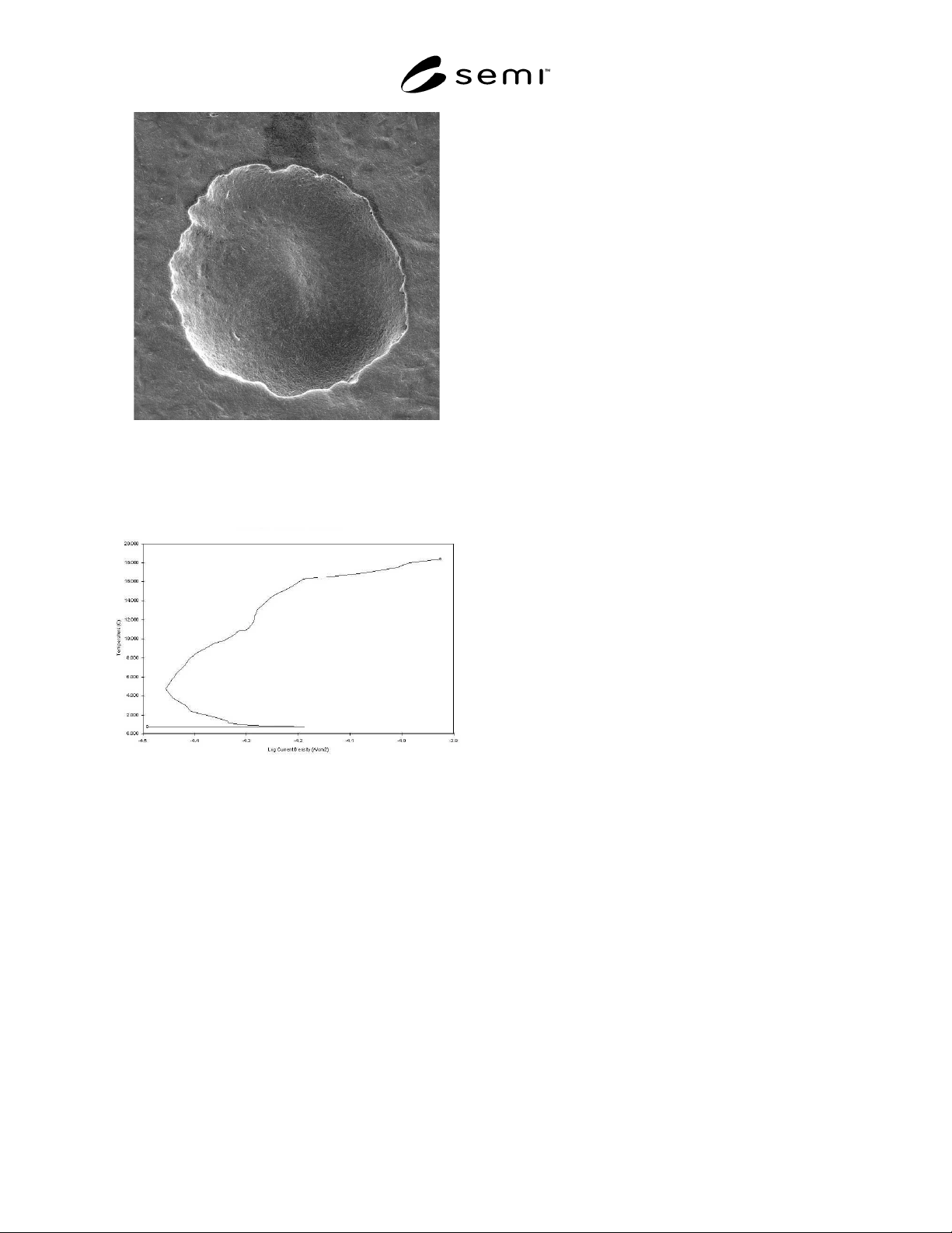
not valid. See Figure A-1.1 for a SEM micrograph of a
typical pit from a valid CPT test.
A1-5.12 Determine critical pitting temperature. The
critical pitting temperature is the temperature at which
the current density exceeds 100 µA/cm
2
for at least 60
seconds. Figure A-1.2 shows an example of a
temperature vs. current density scan. In this particular
example, the critical pitting temperature was
determined to be 18°C.
SEMI F77-0703 © SEMI 2003 6
Figure A-1.1
SEM Micrograph of Pit Formed During CPT
Testing. The Pit is Approximately 100 Microns
Across.
Figure A-1.2
Current Density as a Function of Temperature. The
Critical Pitting Temperature is the Temperature at
Which the Current Density Exceeds 100
µA/cm
2
for
At Least 60 Seconds.
NOTICE: SEMI makes no warranties or
representations as to the suitability of the standards set
forth herein for any particular application. The
determination of the suitability of the standard is solely
the responsibility of the user. Users are cautioned to
refer to manufacturer' s instructions, product labels,
product data sheets, and other relevant literature,
respecting any materials or equipment mentioned
herein. These standards are subject to change without
notice.
By publication of this standard, Semiconductor
Equipment and Materials International (SEMI) takes no
position respecting the validity of any patent rights or
copyrights asserted in connection with any items
mentioned in this standard. Users of this standard are
expressly advised that determination of any such patent
rights or copyrights, and the risk of infringement of
such rights are entirely their own responsibility.
Copyright by SEMI® (Semiconductor Equipment and Materials
International), 3081 Zanker Road, San Jose, CA 95134. Reproduction o
f
the contents in whole or in part is forbidden without express written
consent of SEMI.