semi合集-English.pdf - 第6047页
SEMI G4-0302 © SEMI 1982, 2002 11 A PPENDIX 3 TEST METHOD FOR SLIT STRAIN OF LEA DFRA ME STRIPS USED FOR STA M PING NOTE: T he m aterial in this appendix is an official part of SEMI G4. A 3- 1 Preface A3-1.1 The method i…
SEMI G4-0302 © SEMI 1982, 2002 10
APPENDIX 2
TEST METHOD FOR SLITTER STRAIN OF STRIPS USED FOR
LEADFRAME STAMPING
NOTE: The material in this appendix is an official part of SEMI G4.
A2-1 Preface
This is related to the general evaluation method for
slitter strain of strips used for leadframe stamping. Such
distortion could result in adverse effects on leadframes,
such as coil set, lead twist, and camber.
A2-2 Evaluation Method
A2-2.1 Equipment — Tool microscope (×100).
A2-2.2 Procedure
A2-2.2.1 Collect flat samples approximately 150 mm
in length from strips in a way that residual distortion
can be overlooked. (Collection methods include wire
cutting, etching, refined cutting, etc.) Thickness of
samples should be either 0.25 mm, 0.20 mm, or 0.15
mm.
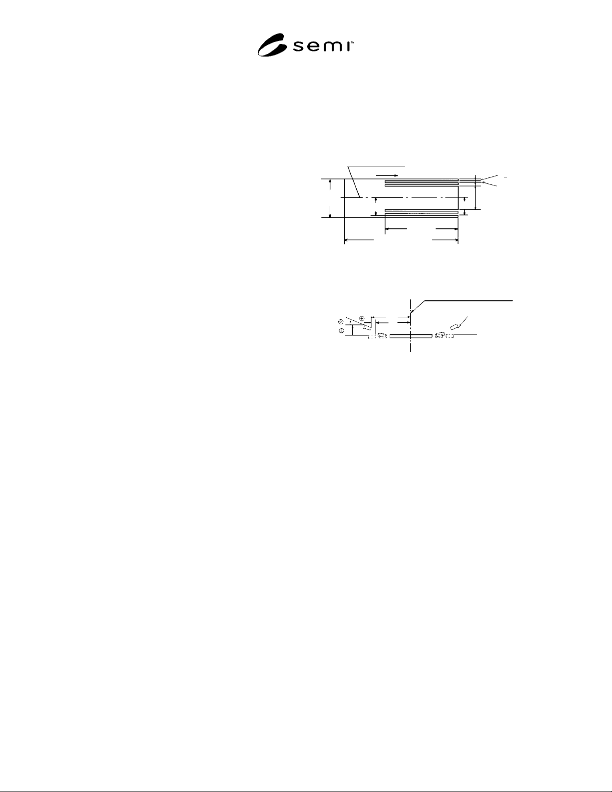
A2-2.2.2 Fashion each sample to the shape shown in
Figure A2-1 by etching or wire cutting. Measure with
the tool microscope to obtain coordinates of the leg end
corner. The reading accuracy is to 0.1 mm (see Note 1).
A2-2.2.3 Using the coordinates of the leg end corner,
for each leg obtain longitudinal curvature “A”, lead
twist “B”, and camber “C”, as shown in Figure A2-2
(see Note 2).
Note 1: Specify the direction of slit burr, and for legs in which
the longitudinal curvature A is reversed, measure by reversing
the sample itself.
Note 2: Measured values are marked as shown in Figure A2-
2.
Note 3: This method should be applied to only slitter strain.
Do not apply to any other kind of strain (e.g., thermal inner
strain).
Base line for
measuring camber
Slit direction
Strip
width
Approx. 150 mm
100 mm
5 mm min.
0.2 ~ 1 mm
2 +
0.5 mm
W
2W
2
Figure A2-1
Shape for Evaluation of Slitter Strain
Base line for measuring camber
Base line for measuring
longitudinal curvature A
Slit burr
Angle B
A
W
1
W
2
Figure A2-2
Evaluation Items
SEMI G4-0302 © SEMI 1982, 2002 11
APPENDIX 3
TEST METHOD FOR SLIT STRAIN OF LEADFRAME STRIPS USED
FOR STAMPING
NOTE: The material in this appendix is an official part of SEMI G4.
A3-1 Preface
A3-1.1 The method is used to evaluate the edge stress caused by slitting.
A3-1.2 This method is applied to thickness between 0.1 mm and 0.3 mm.
A3-2 Evaluation Method
A3-2.1 Equipment — Tool microscope (×100).
A3-2.2 Procedure
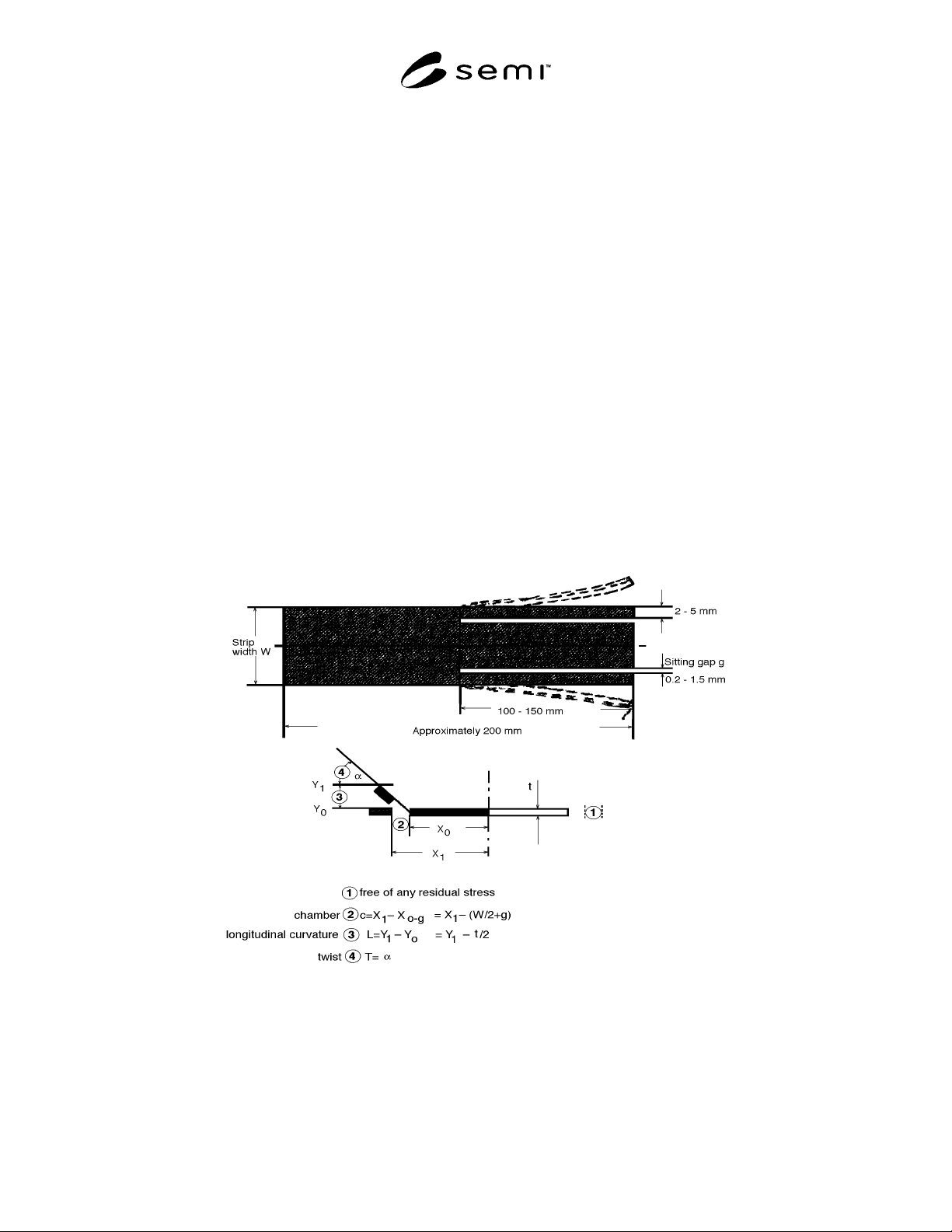
A3-2.2.1 A test piece of approximately 200 mm length is sawn, stamped, etched, wire cut, refined cut, etc., over a
length of 100–150 mm parallel to the rolling direction of a distance of 2–5 mm from the edge of the strip. (See
Figure A1-7.)
A3-2.2.2 The dislocation of the outer strips relative to the plane of the test piece measured as camber c, longitudinal
curvature L, and twist T characterize the internal edge stress. (Note 1)
Note 1: The details of the test method and the maximum admissible values of c, L, and T shall be agreed between purchaser and
supplier.
Figure A1-7
Test Method of Slit Stress

SEMIG4-0302 © SEMI 1982, 2002 12
NOTICE: These standards do not purport to address safety issues, if any, associated with their use. It is the
responsibility of the user of these standards to establish appropriate safety and health practices and determine the
applicability of regulatory limitations prior to use. SEMI makes no warranties or representations as to the suitability
of the standards set forth herein for any particular application. The determination of the suitability of the standard is
solely the responsibility of the user. Users are cautioned to refer to manufacturer’s instructions, product labels,
product data sheets, and other relevant literature respecting any materials mentioned herein. These standards are
subject to change without notice.
The user’s attention is called to the possibility that compliance with this standard may require use of copyrighted
material or of an invention covered by patent rights. By publication of this standard, SEMI takes no position
respecting the validity of any patent rights or copyrights asserted in connection with any item mentioned in this
standard. Users of this standard are expressly advised that determination of any such patent rights or copyrights, and
the risk of infringement of such rights, are entirely their own responsibility.
Copyright by SEMI® (Semiconductor Equipment and Materials
International), 3081 Zanker Road, San Jose, CA 95134. Reproduction o
f
the contents in whole or in part is forbidden without express writte
n
consent of SEMI.