semi合集-English.pdf - 第6084页
SEMI G14-88 © SEMI 198 2, 1996 2 9. Applicable leadf ra me drawing, sh o wing all dimens ions. 5 Dimensions Draw ing mu st show di mens ions for the f ollowing items, if applicable: 1. P ackag e length 2. P ackage w idth…

SEMI G14-88 © SEMI 1982, 19961
SEMI G14-88
GUIDELINE FOR SPECIFYING THE DIMENSIONS AND TOLERANCES
USED TO MANUFACTURE PLASTIC MOLDED DIP PACKAGE
TOOLING
1 Preface
1.1 This document is a guideline for the ordering of
tooling required to mold and form plastic molded DIP
semiconductor packages. It is to be used by packaging
engineers, mold manufacturers, and end-of-line tool
makers as the basis for defining the limits of
manufacturing tolerances.
2 Applicable Documents
2.1 This document specifically refers to:
JEDEC Publication No. 95
1
— JEDEC Registered and
Standard Outline for Semiconductor Devices
2.2 Related information may also be found in:
MIL-STD-100
2
— General Engineering Drawing
Practices
ANSI Y14.5
3
— Dimensioning and Tolerancing
NOTE 1: As listed or revised, all documents cited shall be the
latest publications of adopted standards.
3 Selected Definitions — Pr oduct Criteria
Tolerance Limits
3.1 mismatch and offset — Defined with respect to
package only. All statements will be equally applicable
in two (2) axes. All mismatch and offset measurements
are made after molding and prior to trimming.
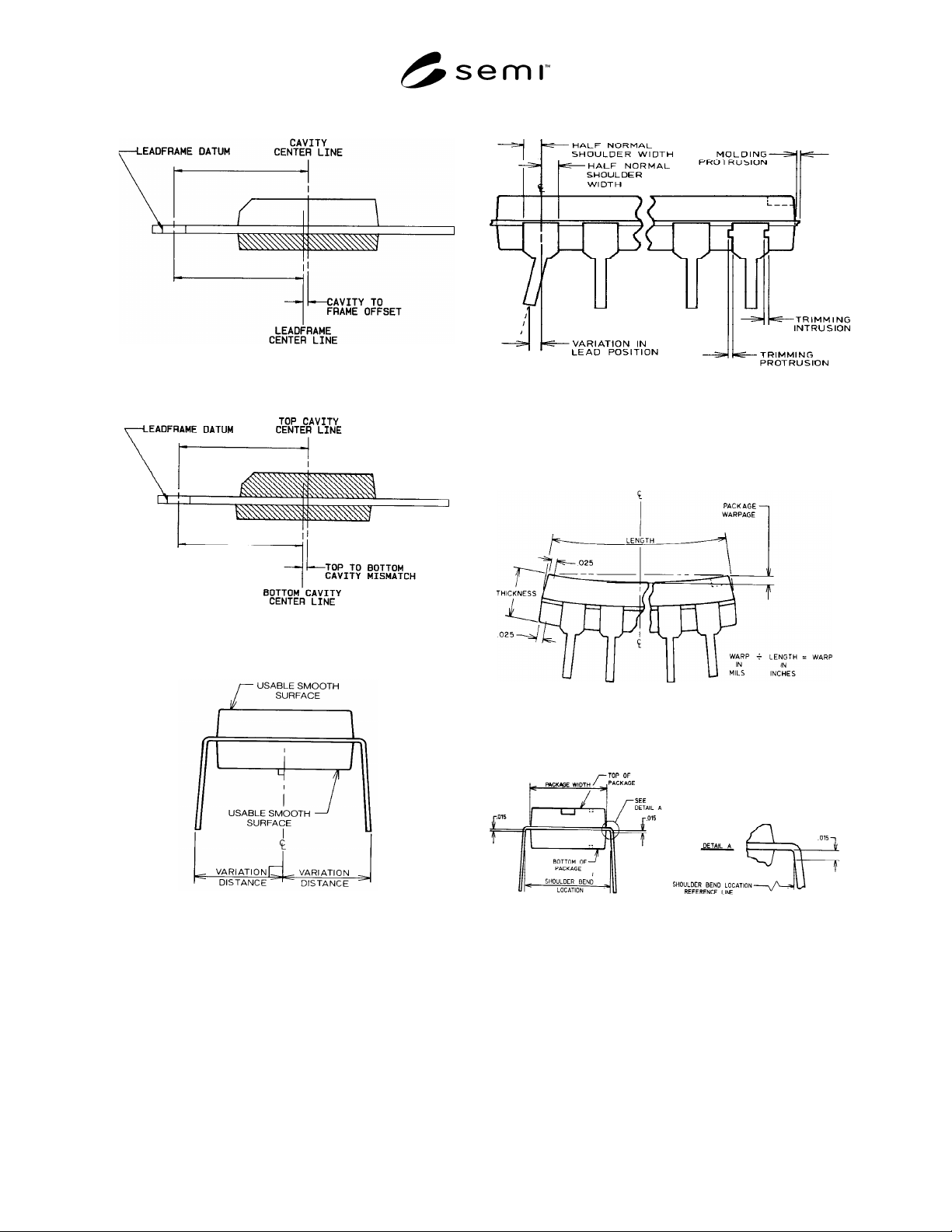
3.1.1 cavity to frame offset — Will be measured prior
to any trimming operation. Offset will be defined as the
difference in bottom cavity position with respect to a
leadframe datum. The offset measurement will exclude
leadframe tolerances. (See Figure 1.)
3.1.2 top to bottom cavity mismatch — Characterized
by the fact that the top and bottom cavities in the mold
are not aligned properly, causing a mismatch condition.
The measurement shall be stated as the difference in the
top cavity position relative to the bottom cavity
position. (See Figure 2.)
1 JEDEC, 20001 Eye Street N.W., Washington, D.C. 20006
2 Military Standards, Naval Publications and Form Center, 5801
Tabor Ave., Philadelphia, PA 19120
3 ANSI, 1430 Broadway, New York, NY 10018
3.2 parting line protrusions — Those plastic excesses
which remain as a normal characteristic after normal
trimming and molding operations. (See Figure 4.)
3.3 top or bottom protrusions — Those plastic
excesses (includes ejector pin “crowns”) which remain
as normal characteristics extending from the smooth
surface of the molded package.
3.4 variations in lead position — Defined with respect
to a 90° angle from the top or bottom of the smooth
surface of the molded package as viewed on the end or
side projections. (See Figure 4.)
3.5 shoulder width intrusions/protrusions — Any
variations in straightness along the defined shoulder
width caused by dambar removal. (See Figure 4.)
3.6 package warpage — Any non-linear dimensional
change from the mold cavity characteristic, usually
caused by incorrect package design or molding
practices. (See Figure 5.)
3.7 shoulder bend location — Measured from the
outermost point of the inner shoulder bend radius. (See
Figure 6.)
4 Ordering Information
Purchase orders for tooling for plastic molded DIP
semiconductor packages furnished to this specification
shall include the following items:
1. A package tooling outline drawing showing all
required dimensions listed in 5. Package surface finish
to be included.
2. A list of any tolerance limits which differ from
the SEMI standards detailed in 6.
3. The type of tooling steel required.
4. The type of leadframe material to be used,
including a drawing.
5. The type of plastic to be molded (if
proprietary, a statement of its shrinkage characteristics).
6. Sampling plan for compliance to 7.
7. The number of spare parts or expendable parts
desired.
8. Type of molding press to be used, including
power requirements.
SEMI G14-88 © SEMI 1982, 1996 2
9. Applicable leadframe drawing, showing all
dimensions.
5 Dimensions
Drawing must show dimensions for the following
items, if applicable:
1. Package length
2. Package width
3. Top cavity thickness
4. Bottom cavity thickness
5. Frame thickness
6. Top ejector pin locations from notch end
7. Bottom ejector pin locations from notch end
8. Ejector size (top and bottom)
9. Ejector depth (top and bottom), draft angle top
side (bottom, side, and end)
10. End notch shape, depth, width, length
11. Pin 1 ID location from package center
12. Pin 1 ID shape and size
13. Corner radius on sides
14. Corner radius on ends
15. Lead spread (nominal) (see Figure 3)
16. Shoulder bend location
17. Shoulder width
6 Product Criteria Dimensional Tolerance
Limits for DIPS
In recognition that every manufacturing process is
subject to variation, the following list details the
acceptable limits of this variation.
8 - 64 LEAD
(unless otherwise noted)
MISMATCH (see Figure 2)
± 0.002"
PACKAGE/FRAME OFFSET (see Figure 1) (excludes
leadframe tolerances)
8-64 ± .002"
PROTRUSIONS (see Figure 4)
Parting line Side and End 0.006"(For reference use
only)
Top Protrusion 0.001"
Bottom Protrusion 0.001"
INTRUSIONS (Ejector Pins)
0.010" maximum
VARIATIONS IN LEAD POSITION (see Figure 4)
0.007" True position
non-accumulative
SHOULDER WIDTH
PROTRUSIONS/INTRUSIONS (see Figure 4)
+ 0.003"/- 0.002"
PACKAGE WARPAGE (see Figure 5)
Warp factor 2.5
SHOULDER BEND LOCATION (see Figure 6)
JEDEC Publication No. 95
outline minus lead thickness.
(Based on balanced plastic.)
LENGTH AND THICKNESS
± 0.002" (see Figure 5)
(Excluding protrusions)
7 Sampling
7.1 Samples used to determine compliance to Section
6 shall be determined between vendor and supplier.
8 Packaging
8.1 Tooling must be packaged in containers designed
and constructed to prevent damage and/or
contamination. Specific protection must be provided if
tooling is to be shipped any great distance.
SEMI G14-88 © SEMI 1982, 19963
Figure 1
Figure 2
Figure 3
Variations from Nominal Lead Location
Figure 4
Parting Line Protrusions and Variation in Lead
Position
Figure 5
Package Warpage and Thickness
Figure 6
Shoulder Bend Location and Package Width