semi合集-English.pdf - 第7241页
SEMI MF525-0705 © SEMI 2003, 2005 4 6.2 The resistivity of the material in the vicinity o f the probe is determined from a calibration curve derived from spreading resistance measurements made under th e same conditions …
SEMI MF525-0705 © SEMI 2003, 2005 3
NOTICE: Unless otherwise indicated, all documents cited shall be the latest published versions.
5 Terminology
5.1 Definitions
5.1.1 effective electrical contact radius, a (cm) — of a spreading resistance probe assembly, an empirical quantity
defined by:
s
R
n
a
4
(1)
where:
n = number of current-carrying probes across which the potential drop is determined,
=
resistivity of a homogeneous semiconductor specimen, ·cm, and
R
s
=
measured spreading resistance, .
5.1.1.1 Discussion — For a three-probe arrangement, n = 1; for a two-probe arrangement, n = 2
5.1.2 epitaxial layer (in semiconconductor technology) — a layer of single crystal semiconducting material grown
on a host substrate that determines its orientation.
5.1.2.1 Discussion — A structure may consist of several epitaxial layers on a substrate: each layer is separated
from a neighboring layer (or the substrate) by an interface region.
5.1.3 spreading resistance, R
s
() — of a semiconductor, the ratio of (1) the potential drop between a small-area
conductive metal probe and a reference point on the semiconductor, to (2) the current through the probe.
5.1.3.1 Discussion — This ratio, in fact, measures metal-to-semiconductor contact resistance as well as classical
spreading resistance for a homogeneous specimen without electrical boundaries in the vicinity of the probes. For a
specimen having resistivity gradients or electrical boundaries, this ratio also includes an effect due to these gradients
or boundaries
5.1.3.2 In a three-probe arrangement, the experimental conditions approximate those of the definition (based on a
single probe) and the spreading resistance R
s
, in , is given by
I
V
R
s
(2)
where:
V = potential drop between one of the current-carrying probes and the reference (non-current carrying) probe on
the front surface, mV, and
I = current through the metal probe, mA.
In a two-probe arrangement, the potential drop, V, is measured between two similar current-carrying probes. In this
case, the voltage-to-current ratio, and hence the spreading resistance, is approximately twice that associated with a
single probe.
5.1.4 substrate (in semiconductor technology) — a wafer that is the basis for subsequent processing operations in
the fabrication of semiconductor devices or circuits.
5.1.4.1 Discussion — The devices or circuits may be fabricated directly in the substrate or in a film of the same or
another material grown or deposited on the substrate..
5.1.5 Other terms relating to silicon technology are defined in SEMI M59.
5.1.6 Terms related to measurement precision are defined in SEMI E89.
6 Summary of Test Method
6.1 The spreading resistance of a reproducibly formed point contact is measured.
SEMI MF525-0705 © SEMI 2003, 2005 4
6.2 The resistivity of the material in the vicinity of the probe is determined from a calibration curve derived from
spreading resistance measurements made under the same conditions on reference specimens of known resistivity.
6.3 The spreading resistance may be measured with the use of one, two, or three probes and (1) by applying a
known constant voltage and measuring the current, (2) by applying a known constant current and measuring the
voltage, or (3) by a resistance comparator technique.
7 Apparatus
7.1 Mechanical Apparatus
7.1.1 Probes and Probe Assembly — A spreading resistance probe assembly with provision for supporting and
lowering either one, two, or three replaceable probe tips to the wafer surface at a reproducible rate and with a
predetermined load. The supporting mechanism shall provide for spatial displacement of the probes for adjustment
of the point of contact.
7.1.1.1 Probe Tip Material — A hard, durable, low-resistance substance that wears well without flaking, such as
osmium, tungsten carbide, or tungsten-ruthenium alloys.
7.1.1.2 Probe Tip Radius — The mechanical radius of curvature of the probe tips in the region that will touch the
specimen shall be less than or equal to 25 m. The tip angle of the probe shall be within the range from 30 to 60°,
inclusive.
7.1.1.3 Probe Loading and Descent Rate — The loading applied to each point shall be less than 50 gf (490 mN).
A 1-mm/s descent rate has been found to be adequate for a 40 gf (390 mN) load (see ¶11.3 and Note 5).
7.1.1.4 Probe Spacing — as used for calibration (see §15).
NOTE 1: Typical probe spacings are between 15 and 1000 m.
7.1.1.5 Probe Insulation — A d-c isolation resistance of 1 G or greater between any pair of probes and between
each probe and any guard circuit used.
7.1.2 Sample Holder — An insulated vacuum chuck or other means for clamping the substrate tightly while
measurements are made.
NOTE 2: The vacuum chuck may be inserted on a high-resolution translatable microscope stage with drum calibrated preferably
in metric units. Gear boxes for stage movement should allow step-size movements in the range from 5 to 500 m per step,
inclusive. Usual increments are 5.0, 10, 25, and multiples of 10 thereof.
7.2 Electrical Measuring Apparatus
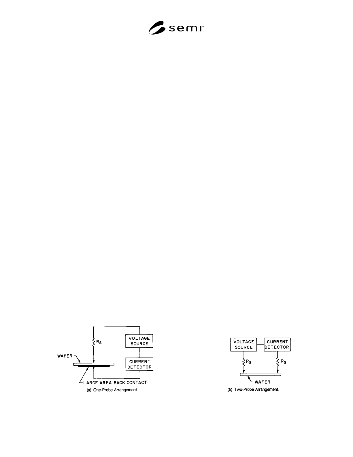
7.2.1 Constant-Voltage Method — Suitable for use with the one- or two-probe arrangement. See Figure 1.
7.2.1.1 D-C Voltage Source — With a constant output between 1 and 20 mV, inclusive. The output potential shall
be constant to within ±0.1% into a load that varies from 1 to 10 M, inclusive.
7.2.1.2 D-C Current Detector — Accurate to within ±0.1% and capable of covering the range from 10 mA to 1 pA,
inclusive.
Figure 1
Electrical Circuits for the Constant-Voltage Method
SEMI MF525-0705 © SEMI 2003, 2005 5
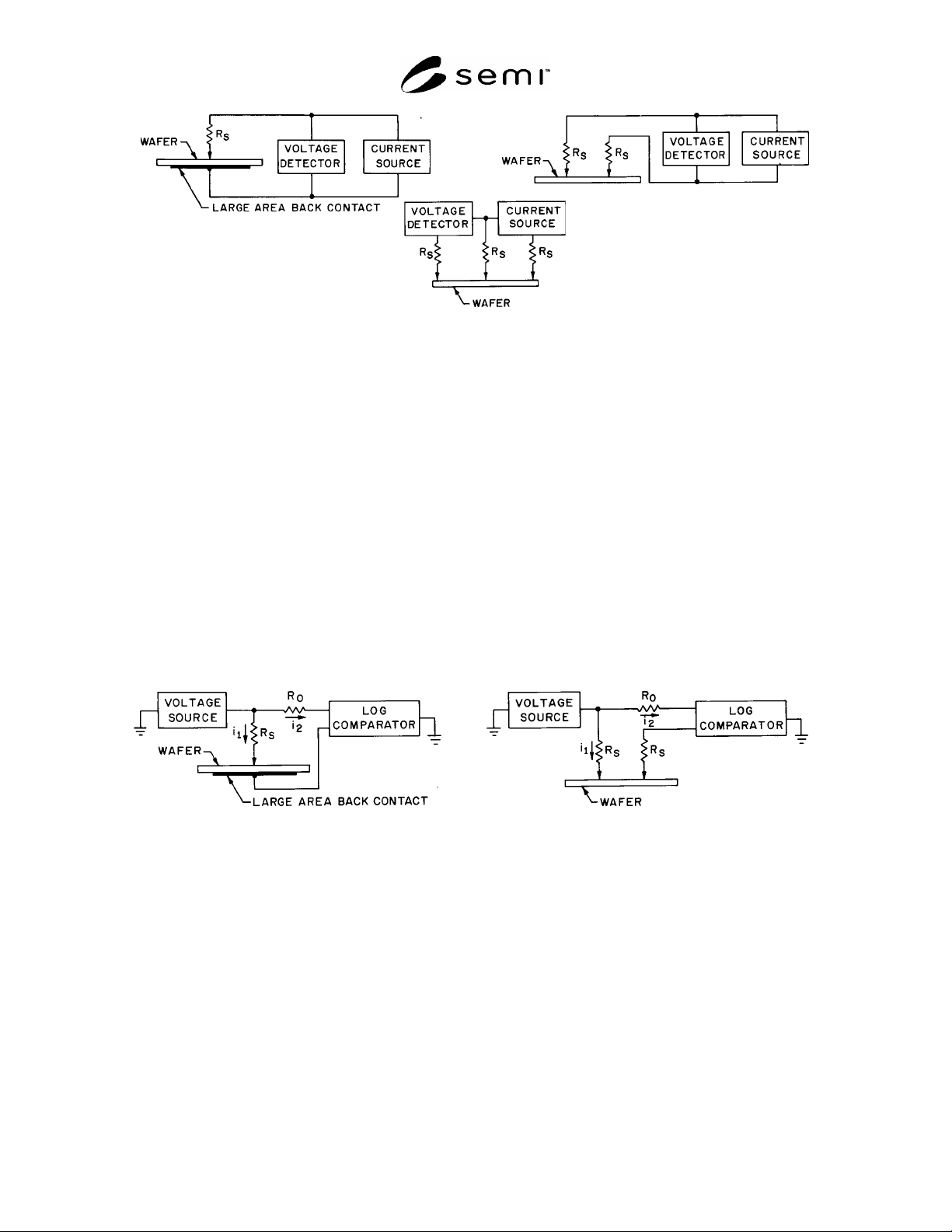
(a) One-Probe Arrangement
(b) Two-Probe Arrangement
(c) Three-Probe Arrangement
Figure 2
Electrical Circuits for the Constant-Current Method
7.2.2 Constant-Current Method — Suitable for use with the one-, two-, or three-probe arrangement. See Figure 2.
7.2.2.1 Variable D-C Current Source — Capable of providing currents from 10 nA to 10 mA, inclusive. The
current source shall be accurate to within ±0.1% and capable of providing a current of 10 nA into a 10M load.
Caution: For safety reasons the compliance voltage shall not exceed 40 V.
7.2.2.2 D-C Voltage Detector — Linear over the range from 1 to 100 mV, inclusive, and accurate to within ±0.1%
of the reading. The input impedance shall be 10 M or greater.
7.2.3 Comparator Method — Suitable for use with the one- or two-probe arrangement. See Figure 3.
7.2.3.1 D-C Voltage Source, with a constant output between 1 and 20 mV, inclusive, but no special requirements
on the precision.
7.2.3.2 Log Comparator — With an output voltage proportional to the logarithm of the ratio of two currents.
Together with its standard resistor, R
0
, the comparator shall be capable of measuring resistances from 1 to 10 M
inclusive, with a deviation from linearity not greater than ±1%.
(a) One-Probe Arrangement (b) Two-Probe Arrangement
Figure 3
Electrical Circuits for the Log Comparator Method
7.2.3.3 Standard Resistor — Nominally 10 k, known to an accuracy of ±0.1%.
7.3 Microscope — Capable of a magnification of at least 400×.
7.4 Thermometer — An ASTM Precision Thermometer having a range from 8 to +32°C, inclusive, and
conforming to the requirements for Thermometer 63C as described in ASTM Specification E 1.
8 Reagents and Materials
8.1 Resistivity Standards for Calibration
8.1.1 Resistivity standards shall be chosen from substrates in the resistivity range of the unknowns in accordance
with §12.