semi合集-English.pdf - 第4497页
SEMI D19-0305 © SEMI 1999, 2005 4 10.6.2.3 Repeat ¶¶10.6.2 .1 and 10.6.2 .2 on the same location of th e sample. 10.6.2.4 Calculate color difference for each colored layer in the L*a*b* col o r system or the L*u*v* color…
SEMI D19-0305 © SEMI 1999, 2005 3
8.2 This standard may involve hazardous materials, operations and equipment. This standard does not purport to
address all of the safety problems associated with its use. It is the responsibility of the user of this standard to
establish appropriate safety and health practices and determines the applicability of regulatory limitations prior to
use.
9 Samples
9.1 FPD color filters are used as samples. For HCl resistance tests, color filters without ITO should be used.
NOTE 1: The test report shall identify whether or not ITO is present on the sample.
10 Procedure
10.1 Pour the selected chemicals into a test container.
10.2 Adjust the temperature of the chemicals to a predetermined value.
10.3 Place the sample, film side up, into the chemicals and cover the test container to prevent chemical evaporation.
10.4 Leave the sample in the chemicals for a predetermined period of time.
10.5 Remove the sample from the chemical bath. Completely remove all chemicals remaining on the sample.
NOTE 2: For chemicals, temperature and soaking time, refer to §8, Reagents and Test Conditions.
10.6 Evaluate the sample condition according to the following criteria:
10.6.1 Change of Appearance — During each test, observe any change of appearance, e.g., wrinkles, cracks, change
of surface conditions due to swelling, film peeling, and discoloration. The sample is compared with untreated
sample. Various observation techniques can be employed, including the following which is included for reference
only:
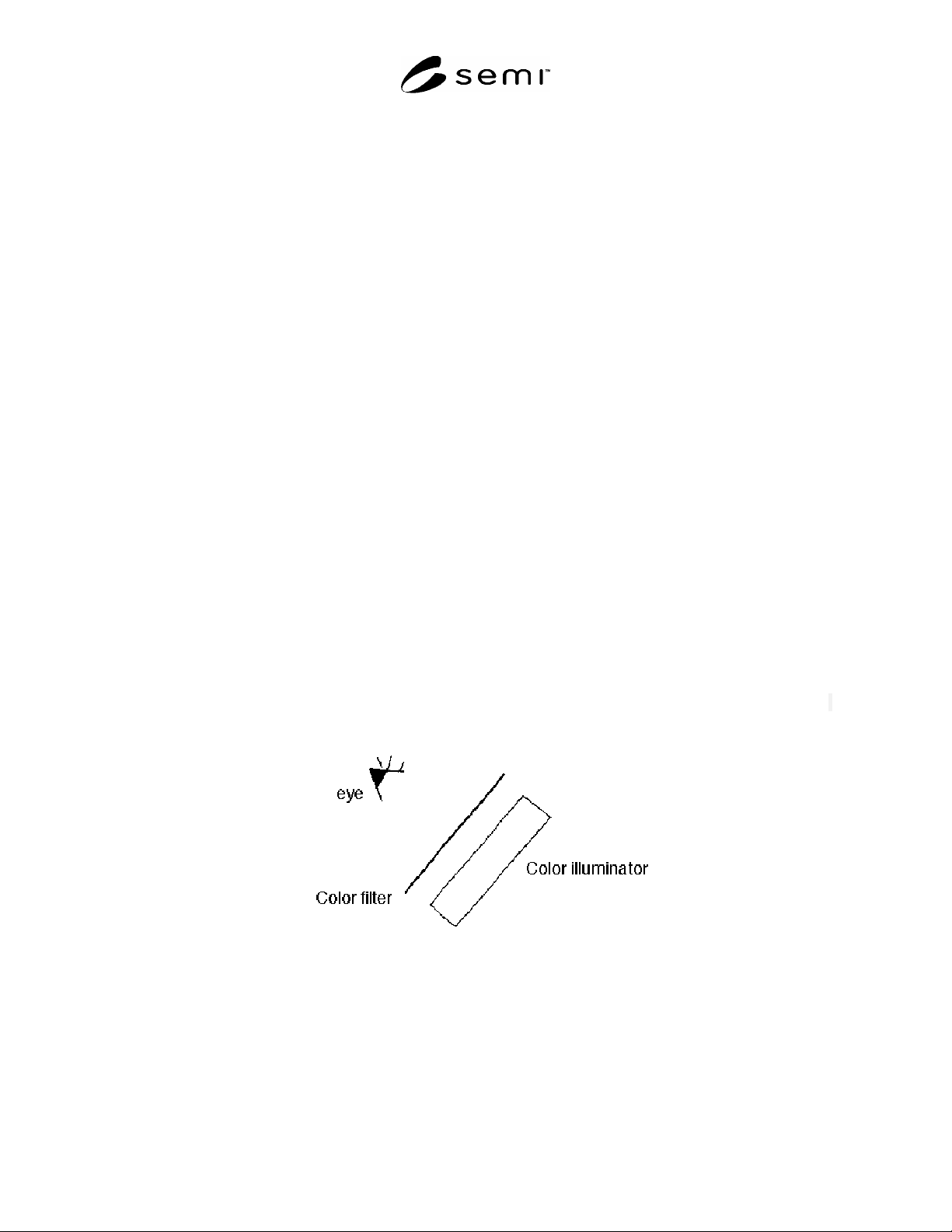
10.6.1.1 Visual observation of transmission of the color filter by use of a color illuminator (Figure 1).
10.6.1.2 Visual observation of reflectance of the film side of the color filter by use of a floodlight.
10.6.1.3 Microscope observation or transmission of a color filter by use of transmitted illumination.
10.6.1.4 Microscope observation of reflectance of the color filter by use of reflected illumination.
10.6.1.5 A surface profiler (stylus type) is used in order to measure the changes of film thickness of the color filter.
Figure 1
Visual Observation of Transmission of a Color Filter by Use of a Color Illuminator
10.6.2 Color Differences
10.6.2.1 Measure transmitted spectra of each colored layer of the color filter at any location. The center area of the
sample is recommended.
10.6.2.2 Calculate tri-stimulus values of each colored layer of the color filter in accordance with JIS Z8730.

SEMI D19-0305 © SEMI 1999, 2005 4
10.6.2.3 Repeat ¶¶10.6.2.1 and 10.6.2.2 on the same location of the sample.
10.6.2.4 Calculate color difference for each colored layer in the L*a*b* color system or the L*u*v* color
specification system from the tri-stimulus values measured before and after this test, according to the method
specified in JIS Z8730. Calculate either the difference E*ab or E*uv as the amount of color change of the color
filter.
NOTE 3: Both the L*a*b* and L*u*v* color specification system can be used to evaluate the color change.
11 Report
11.1 Report the following:
11.1.1 Report date
11.1.2 Test date
11.1.3 Ambient temperature, in
o
C
11.1.4 Conditions of the sample (construction of FPD color filter) – presence or absence of ITO film
11.1.5 Test conditions (name of chemicals, concentration, temperature and volume of chemicals, soaking time)
11.1.6 Observed changes in sample appearance between, before, and after the test.
11.1.7 The calculated color differences, for measurement location on each sample, and the color system used for
these calculations.
12 Precision and Accuracy
12.1 No test data currently exists on which to base these statements. Tests are planned to develop such data for both
single-laboratory repeatability and multi-laboratory reproducibility, on samples of the same nominal characteristics,
and across a range of nominal characteristics.
NOTICE: SEMI makes no warranties or representations as to the suitability of the standards set forth herein for any
particular application. The determination of the suitability of the standard is solely the responsibility of the user.
Users are cautioned to refer to manufacturer's instructions, product labels, product data sheets, and other relevant
literature, respecting any materials or equipment mentioned herein. These standards are subject to change without
notice.
By publication of this standard, Semiconductor Equipment and Materials International (SEMI) takes no position
respecting the validity of any patent rights or copyrights asserted in connection with any items mentioned in this
standard. Users of this standard are expressly advised that determination of any such patent rights or copyrights, and
the risk of infringement of such rights are entirely their own responsibility.
Copyright by SEMI® (Semiconductor Equipment and Materials
International), 3081 Zanker Road, San Jose, CA 95134. Reproduction of
the contents in whole or in part is forbidden without express written
consent of SEMI.
SEMI D20-1000 © SEMI 1993, 20001
SEMI D20-1000
DEFECT TERMINOLOGY FOR FLAT PANEL DISPLAY MASKS
This terminology was technically approved by the Global Flat Panel Display Committee and is the direct
responsibility of the Japanese Flat Panel Display Materials and Components Committee. Current edition
approved by the Japanese Regional Standards Committee on July 28, 2000. Initially available on SEMI
OnLine September 2000; to be published October 2000. Originally published in 1993.
1 Purpose
1.1 This document defines defect terminology for FPD
masks. By this standard, it is intended that the concepts
of terms which should be used at the technical
conferences, business discussion, etc are clarified and
that standardization as to masks will be promoted.
2 Scope
2.1 These terms apply to photomasks that are
principally used in fabricating flat panel display.
2.2 These definitions do not purport to address safety
issues, if any, associated with their use. It is the
responsibility of the user of these definitions to
establish appropriate safety and health practices and
determine the applicability of regulatory limitations
prior to use. SEMI makes no warranties or
representations as to the suitability of the definitions set
forth herein for any particular application. The
determination of the suitability of the definitions is
solely the responsibility of the user. Users are cautioned
to refer to manufacturer’s instructions, product labels,
product data sheets, and other relevant literature
respecting any materials mentioned herein. These
definitions are subject to change without notice.
3 Referenced Documents
None.
4 Terminology
4.1 pin hole — a small hole-shaped opening defect on
the chrome-pattern.
4.2 intrusion — an absence of chrome extending
inward from boundary.
4.3 pattern disconnect — an intrusion which
completely separates the continuity of the chrome-
pattern.
4.4 missing pattern image — comp lete disappearance
of the designed chrome-pattern.
4.5 spot — isolated chrome residue on the etched area.
4.6 protrusion — an extension of chrome beyond the
desired boundary.
4.7 bridge — an extension of chrome which connects
completely and continuously from an edge to another
edge.
4.8 edge roughness — subtle roughness and/or jagged
zone on the pattern edge.
4.9 round of corner — unintended round on the
pattern corner.
4.10 flaw
4.10.1 scratch — relatively thick and deep linear
friction defect on the surface of the glass.
4.10.2 sleek — extremely thin and light linear friction
defect on the surface of the glass.
4.10.3 pit — small dot-shaped depression on the
surface of the glass.
4.11 chipping — chipping of edge of the glass caused
by cutting or treatment.
4.12 bubble — void in the interior of the glass
substrate.
4.13 foreign substance
4.13.1 particle — relatively high foreign substance
attached on the surface of the substrate.
4.13.2 contamination — cluster of relatively small
substances attached on the surface of the substrate in
the shape of thin film.