semi合集-English.pdf - 第7334页
SEMI MF1389-0704 © 2004 2 3 Limitations 3.1 Variations in Excitation Inten sity — The extrinsic bound exciton (BE) and in trinsic free exciton (FE) luminescence features do not va ry at the same rate with excitation inte…

SEMI MF1389-0704 © 2004 1
SEMI MF1389-0704
TEST METHODS FOR PHOTOLUMINESCENCE ANALYSIS OF SINGLE
CRYSTAL SILICON FOR III-V IMPURITIES
This guide was technically approved by the Global Silicon Wafer Committee and is the direct responsibility
of the North American Silicon Wafer Committee. Current edition approved for publication by the North
American Regional Standards Committee on March 14, 2004. Initially available at
www.semi.org
May
2004; to be published July 2004. Original edition published by ASTM International as ASTM F 1389-92.
Last previous edition SEMI MF1389-00.
1 Purpose
1.1 Electronic-grade polycrystalline silicon producers
and users require information regarding impurities for
quality assurance as well as for research and
development purposes. Polysilicon is float-zoned and a
sample from the zoned rod is analyzed following these
test methods to obtain impurity densities that can be
related to the impurity content of the starting material
(see SEMI MF1723).
1.2 Photoluminescence analysis identifies and
quantifies the electrically active dopant impurities in
monocrystalline silicon. These test methods address
boron, phosphorus, arsenic, and aluminum, found as
impurities in electronic grade silicon.
1.3 These test methods can be applied to doped and
undoped float-zoned or Czochralski material.
2 Scope
2.1 These test methods cover the simultaneous
determination of electrically active boron, phosphorus,
arsenic, and aluminum content in low-dislocation
monocrystalline silicon.
NOTE 1: These chemical species can also be determined by
the low temperature infrared analysis procedure of SEMI
MF1630.
2.2 These test methods can be used for samples that
have dopant densities between approximately 1 × 10
11
and approximately 5 × 10
15
atoms/cm
3
.
2.3 The concentrations obtained using these test
methods are based on an empirically determined
relationship of the logarithm of the concentration to the
logarithm of specific luminescence line-intensity ratios.
2.4 The empirical relationship established assumes a
constant sample excitation level for all measurements
on a given instrument.
2.5 To accommodate differences in instrumentation,
two methods are included. Test Method A refers to
procedures appropriate for dispersive infrared
spectrophotometers operating under the high sample
excitation conditions and Test Method B refers to
procedures appropriate for Fourier transform
instruments operating under low excitation conditions.
2.5.1 Typical calibration curves for each test method
are provided. These curves are modified for each
instrument using the analysis of standard samples as
reference data. Once modified, the curves for a given
instrument should produce sample dopant density
values that agree with other similarly operated
instruments using the same test method. Data obtained
using Test Method A may not agree with data obtained
using Test Method B, hence values must be reported
with reference to the test method used.
NOTE 2: Several different methods of photoluminescence
analysis are currently in practice worldwide. These test
methods address two of these, one (Test Method A) in use
primarily in Japan
1
and the other (Test Method B) primarily in
the United States. Recently published works
2,3
describe other
approaches.
2.6 Many laboratories use photoluminescence to
analyze epitaxial layers. However this application
encounters many variables and the underlying physics
is not fully understood; hence these test methods do not
attempt to outline standard practices regarding such
analysis.
NOTICE: This standard does not purport to address
safety issues, if any, associated with its use. It is the
responsibility of the user of this standard to establish
appropriate safety and health guides and determine the
applicability of regulatory or other limitations prior to
use.
1 Test Method A is essentially equivalent to JIS H 0615, Test
Method for Determination of Impurity Concentrations in Silicon
Crystal by Photoluminescence Spectroscopy. This standard is
available from Japanese Standard Association 1-24, Akasaka 4
Chome, Minato-ku, Tokyo 107-0000, Japan. Telephone: 81-(0)3-
3583-8005; Fax: 81-(0)3-3586-2014; Website:
www.jsa.or.jp
.
2 Colley, P. McL., and Lightowlers, E. C., “Calibration of the
Photoluminescence Technique for Measuring B, P, and Al Concen-
trations in Silicon in the Range 1e12 to 1e15 at/cm 3 Using Fourier
Transform Spectroscopy,” Semiconductor Science and Technology 2,
157–166 (1987).
3 Schumacher, K. L., and Whitney, R. L., J. Electron. Materials
18(6), 681–687 (1989).

SEMI MF1389-0704 © 2004 2
3 Limitations
3.1 Variations in Excitation Intensity — The extrinsic
bound exciton (BE) and intrinsic free exciton (FE)
luminescence features do not vary at the same rate with
excitation intensity.
4
The FE features increase
proportionally with excitation intensity, while the BE
features increase proportionally at low excitation levels
but become more slowly increasing at higher excitation
levels generally above the electron hole droplet (EHD)
onset point. Since the calculated concentrations are
derived from the ratio of extrinsic features to the
intrinsic feature, the ratio will be decreasing as the
excitation intensity is increasing. Thus, if a sample is
measured at a higher excitation level than the
instrument is calibrated for, the calculated
concentration will be artificially low, and vice versa.
3.2 Sample surface damage, bulk defects, or other
lifetime reducers also affect the line-intensity ratios and
overall luminescence intensity owing to their tendency
to reduce the steady state population of excitons, thus
mimicking the effects of a lower excitation intensity.
Other mechanisms related to the presence of these
defects may also introduce decalibrating effects. Some
luminescence features are generated by defects; for
example, those at 6510 and 7050 cm
−1
are typical of
thermally stressed samples. Such features can provide
qualitative information about the presence of defects.
5,6
3.3 The ratios and line widths of the silicon
luminescence features vary strongly with temperature,
hence variations in sample temperature must be
avoided. Corrections for the effects of temperature
variations are included in these test methods (see
Section 7.1).
3.4 Overlapping Spectral Features
3.4.1 The boron B
TO
(BE) feature at 8812.6 cm
−1
overlaps the P
TO
(b′
1
) feature at 8812.7 cm
−1
causing a
direct error when calculating boron concentration. The
beta-series P
TO
(b′
1
) line is approximately one-tenth the
intensity of the alpha series P
TO
(BE) line at 8806.6
cm
−1
, so a subtraction based on the amount of
phosphorus present can be made in the boron feature
measurement. An alternative approach is to use the
B
TO
(b
1
) boron line, which is free from a coincident
4 Nakayama, H., Nishino, T., and Hamakawa, Y.,“Analysis of the
Excitation Luminescence of Silicon for Characterization of the
Content of Impurities,” Jap. J. Appl. Phys. 19(3), 501–511, (1980).
5 Drozdov, N. A., Patrin, A. A., and Tkachev, V. D.,
“Recombination Radiation on Dislocations in Silicon,” Soviet
Physics, J.Experimental and Theoretical Physics 23(11), 597 1976).
6 Suezawa, M., Sasaki, Y., Nishina, Y., and Sumino, K., “Radiative
Recombination on Dislocations in Silicon Crystals,” Jap. J. Appl.
Phys. 20(7), L537 (1981).
phosphorus line, provided the instrument has been
calibrated for this feature.
3.4.2 The antimony Sb
TO
(BE) line falls between the
boron and phosphorus transverse optical (TO) features.
Since the line widths are broad relative to the line
positions of these features, the presence of antimony
affects the apparent intensities of boron and phosphorus
TO features. The no-phonon, (NP) features for these
elements could be used providing the instrument is
calibrated for them.
3.4.3 In general, the broad TO phonon region features
can interfere, particularly when a sample contains
widely differing levels of impurities. For example,
when boron greatly exceeds phosphorus, the P
NP
(BE)
line must be used, and when phosphorus greatly
exceeds boron, one of the approaches described in
Section 3.4.1 must be used.
3.5 Stress in samples can cause NP region feature
splitting and thus affect the established TO/NP line
ratio for a given impurity. The concentrations
calculated from such spectra would be artificially low.
Peak area calculation methods reduce the
measurement' s sensitivity to line splitting effects.
3.6 The calibration curves presented in these test
methods are traceable to resistivity measurements (see
SEMI MF723), neutron transmutation doped, (NTD)
reference material, and low-temperature infrared
absorption spectroscopy (FT-IR) measurements (as a
secondary standard) (see SEMI MF1630). Hence
inaccuracies in the work that produced the calibration
curves impact the accuracy of the PL results.
4 Referenced Standards
4.1 SEMI Standards
SEMI C28 — Specifications and Guidelines for
Hydrofluoric Acid
SEMI C30 — Specifications and Guidelines for
Hydrogen Peroxide
SEMI C35 — Specifications and Guideline for Nitric
Acid
SEMI MF723 — Practice for Conversion Between
Resistivity and Dopant Density for Boron-Doped,
Phosphorus-Doped, and Arsenic-Doped Silicon
SEMI MF1630 — Test Method for Low Temperature
FT-IR Analysis of Single Crystal Silicon for III-V
Impurities
SEMI MF1723 — Practice for Evaluation of
Polycrystalline Silicon Rods by Float-Zone Crystal
Growth and Spectroscopy
SEMI MF1389-0704 © 2004 3
4.2 ASTM Standard
D 5127 — Guide for Ultra Pure Water Used in the
Electronics and Semiconductor Industry
7
NOTICE: Unless otherwise indicated, all documents
cited shall be the latest published versions.
5 Terminology
5.1 Definitions
5.1.1 defect luminescence lines — those features arising
from defect structures in the silicon.
5.1.2 electron hole droplet (EHD) — the condensed
phase (liquid) of the excitonic gas generated by
photoexcitation.
5.1.2.1 Discussion — The exciton population is
dependent upon excitation intensity and can be raised to
the point where the exciton density is sufficient to allow
condensation of the exciton gas into a liquid like
exciton state.
8
The existence of EHD luminescence can
be an indirect measurement of excitation power density
on the sample.
5.1.2.2 EHD onset occurs at the point in the sample
excitation intensity curve where the electron-hole-
droplet begins to form.
9
The EHD luminescence
includes a very broad feature underlying the TO region
impurity lines which, with increasing excitation
intensity, both intensifies and shifts to lower energies
relative to the other silicon luminescence features.
5.1.3 excitons — the electron-hole pairs that give rise to
the luminescence of interest upon recombination at
either a free lattice site (free exciton) or an impurity
atom site (bound exciton).
5.1.4 extrinsic line (X
TO
(BE) or X
NP
(BE)) — the
luminescence that arises from an exciton captured by an
impurity site in the crystal lattice (a bound exciton).
5.1.4.1 Discussion — Its energy is lower than the
intrinsic emission by an amount related to the exciton
binding energy of the impurity at 4.2 K. “X” is the
impurity element symbol and “BE” indicates bound
exciton luminescence line. Extrinsic luminescence also
includes features attributed to bound multi-exciton
complexes (b
1
, b
2
, or b
3
would indicate the first, second
and third bound multi-exciton complex lines,
respectively). In donor luminescence, these complexes
7 Annual Book of ASTM Standards, Vol 11.01, ASTM International,
100 Barr Harbor Drive, West Conshohocken, PA 19428. Telephone:
610-832-9500, Fax: 610-832-9555, Website:
www.astm.org.
8 Nakashima, H., and Shiraki, Y., “Role of Shallow Impurities and
Lattice Defects in Nucleation of Electron-Hole Droplets in Si,” Solid
State Comm. 40, 195–197 (1981).
9 Hammond, R. B., and Silver, R. N., “Onsets of the Electron-Hole
Droplet Luminescence in Si,” Phys. Rev. Lett. 42(8), 523–526 (1979).
give rise to two series of lines in the TO region, called
the alpha and beta series. The weaker beta series
features are denoted by an apostrophe after the line
notation (that is, P
TO
(b′
1
)). See Table 1 and Table 2 for
line locations.
5.1.5 intrinsic line (I
TO
(FE)) — the luminescence that
arises from the silicon itself, with no impurity species
affecting the exciton recombination.
10,11
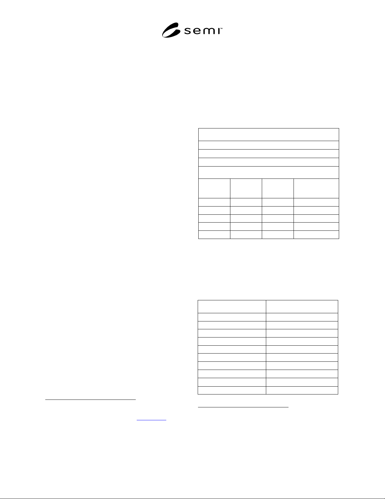
Table 1 Photoluminescence Line Locations
(Vacuum Wavenumbers)
Silicon Free Exciton (FE) Lines:
I
TO
(FE) at 8848 cm
−1
I
LO
(FE) at 8860 cm
−1
I
TA
(FE) at 9166 cm
−1
Major Shallow Impurity Bound Exciton (BE) Lines:
Element
TO region,
cm
−
1
NP region,
cm
−
1
NP/TO region BE
line intensity ratio
A
Boron 8812.6 9281.3 0.017
(Antimony) (8810.5) (9280.0) (0.010)
Phosphorus 8806.8 9275.4 1.4
Aluminum 8803.4 9271.8 0.7
Arsenic 8801.0 9269.4 2.0
NOTE 1: To convert vacuum wavenumbers to air wavenumbers:
air wavenumber = 1.00030025 × vacuum wavenumber
NOTE 2: To convert wavenumbers to electronvolts:
eV = 1.23985 × 10
−4
× wavenumber
A
Instrument resolution = 0.5 cm
−1
, sample = FZ silicon.
Table 2 Photoluminescence Line Locations
(Vacuum Wavenumbers) Detailed Listing for Boron
and Phosphorus
Boron Features, cm
−
1
Phosphorus Features, cm
−
1
B
NP
(BE) = 9281.3 P
NP
(BE) = 9275.4
B
NP
(b
1
) = 9263.6 P
NP
(b
1
) = 9246.4
B
NP
(b
2
) = 9245.9 P
NP
(b
2
) = 9223.9
P
NP
(b
3
) = 9208.4
P
NP
(b
4
) = 9197.8
B
TA
(BE) = 9130.1 P
TA
(BE) = 9124.4
B
TA
(b
1
) = 9112.4 P
NP
(BE-2e) = 8992.8
A
B
TA
(b
2
) = 9095.2
B
TO
(BE)= 8812.6
P
TO
(b
1
′) = 8812.7
B
B
TO
(b
1
) = 8795.0 P
TO
(BE) = 8806.8
C
10 Tajima, M., “Determination of Boron and Phosphorus Concen-
tration in Silicon by Photoluminescence Analysis,” Appl. Phys. Lett.
32(11), 719 (1978).
11 Tajima, M., “Quantitative Impurity Analysis in Si by the Photo-
luminescence Technique,” edited by J. Nishizawa, Japan Annual
Reviews in Electronics, Computers, and Telecommunications—
Semiconductor Technology (OHM—North Holland, 1982).