semi合集-English.pdf - 第6201页
SEMI G42-0996 © SEMI 1986, 2004 4 Figure 1 Thermal Test Board — Dual In-Line P ackage (Unit: mm) 1. Materi al — Epoxy Glass 1.52–1.65 mm thic kness, FR- 4 (Green). Co pper Clad. 28.3 g (1 Oz.) 1/1 2. Gold-Plat ed Fingers…

SEMI G42-0996 © SEMI 1986, 2004 3
Table 2 Trace Dimension for BGA Package Boards
Pad Pitch (mm)
Trace Radius, R (mm)
Solder Mask Opening
Diameter Ø1 (mm)
Hole Diameter Ø 2 (mm)
Number of Pads
1.5 0.9 0.6 0.2 33 x 33
1.27 0.8 0.6 0.35 39 x 39
1.0 0.6 0.45 0.3 49 x 49
6.1.2.2.6 Equivalent boards for other packages should
follow guidelines similar to those described in Sections
6.1.2.2.1–6.1.2.2.5.
6.1.2.2.7 Multi-Layer Board — When measuring
thermal resistance using a multi-layer board, the layer
shall be constructed as shown in Figure 9. The inner
pattern should have the clearance as shown in Figure 10
to isolate with via holes.
6.1.3 Mounting Guidelines
6.1.3.1 Example of package mounting on the boards is
shown in Figures 11 and 12. Packages should be
mounted such that the center line of the test board is
coincidental with the center line of the package.
6.1.3.2 For DIP and CCP, the longer edge of the
package should be closest to the long edge of the board.
6.1.3.3 For QFP, PGA, and BGA package board, the
package should be mounted in the center of the board.
6.1.3.4 Packages must be mounted such that the
standoff height above the board is as per JEDEC
guidelines. In the case of a new package without such
information available, a minimum of 0.127 mm (5 mil)
air gap between the bottom surface of the package and
the thermal test board is acceptable.
6.1.4 Mounting the Test Board for Still-Air R
θJA
Measurement
6.1.4.1 The test board should be mounted on a clamp
as shown in Figure 13 through a suitable edge
connector clamp.
6.1.4.2 The test board and the edge connector clamp
are placed in a 0.0283 m
3
(one cubic foot) enclosure as
shown in Figure 13. The edge connector clamp height
must be adjusted to ensure positioning of the package in
the center of the chamber.
6.1.4.3 The electrical wire connections from the
package are routed out of the one cubic foot enclosure
either through an edge connector or through small
diameter holes in the box.
6.1.5 Mounting the Test Board for Forced-Air R
θJA
Measurement — Forced air R
θJA
measurements are
performed in a wind tunnel whose diameter is 203.2
mm (8.00 inches). Details of the wind tunnel are given
in SEMI G38.
6.1.5.1 The test board should be mounted inside the
wind tunnel on an edge connector clamp as shown in
Figure 14.
6.1.5.2 The test board is placed in the wind tunnel such
that the longer edge of the package is in a vertical
position (see Figure 14).
6.1.5.3 The longer edge of the package should face the
direction of air flow.
6.1.5.4 The longer side of the package must meet the
air front first, as shown in Figure 14.
6.1.5.5 Air may be forced through the wind tunnel by
either blowing from one end or by suction. (Suction
being preferred.)
6.1.5.6 The test board and the edge connector clamp
are placed in the wind tunnel as shown in Figure 14.
The edge connector clamp height must be adjusted to
ensure positioning of the package in the center of the
wind tunnel.
6.1.6 Thermal Resistance Measurement Methods —
Methods for measuring R
θJA
(Junction-to-Ambient
Thermal Resistance) of IC packages using thermal test
chips have been described in SEMI G32 and SEMI
G38, respectively. These methods or equivalent
methods such as the use of switching techniques, as
described in MIL-STD-883C, Method 1021.1, should
be used for making thermal resistance measurements of
IC packages using thermal test chips or IC devices.
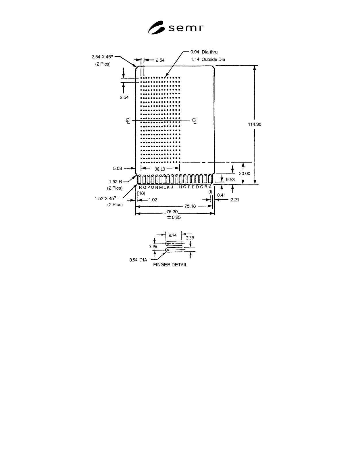
SEMI G42-0996 © SEMI 1986, 2004 4
Figure 1
Thermal Test Board — Dual In-Line Package
(Unit: mm)
1. Material — Epoxy Glass 1.52–1.65 mm thickness, FR-4 (Green). Copper Clad. 28.3 g (1 Oz.) 1/1
2. Gold-Plated Fingers — 0.8 µm Min. Thickness, 18 on Each Side
3. Fabricate — IPC-D-320, Class III
4. Tolerance — ± 0.1 mm (Unless noted)
5. Fingers on Component Side of Board — Designed as A thru R, Fingers on Solder Side of Board — Designated
as 1 thru 18 (with 18 at Right When Viewing Face of Board)
6. All Holes Plated Thru
7. Mates with Dale Connector Part Number EB 7D-A18GFX or Equivalent
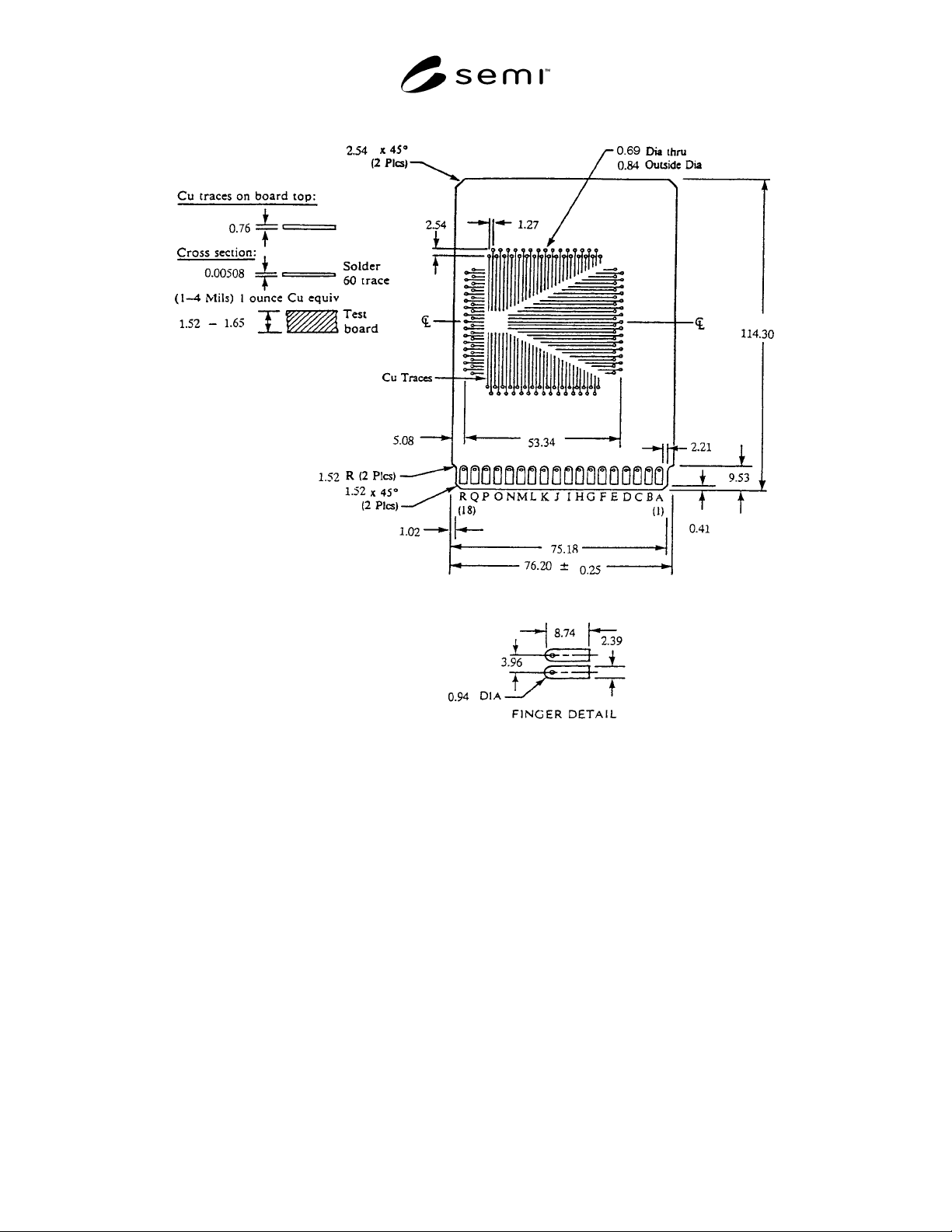
SEMI G42-0996 © SEMI 1986, 2004 5
Figure 2
Thermal Test Board — PCC Packages
Unit: mm
1. Material — Epoxy Glass 1.52–1.65 mm thickness, FR-4 (Green). Copper Clad. 28.3 g (1 Oz.) 1/1
2. Gold-Plated Fingers — 0.8 µm Min. Thickness, 18 on Each Side
3. Fabricate — IPC-D-320, Class III
4. Tolerance — ± 0.1 mm (Unless noted)
5. Fingers on Component Side of Board — Designed as A thru R, Fingers on Solder Side of Board — Designated
as 1 thru 18 (with 18 at Right When Viewing Face of Board)
6. All Holes Plated Thru
7. Mates with Dale Connector Part Number EB 7D-A18GFX or Equivalent