semi合集-English.pdf - 第934页
SEMI E119-1104 © SEMI 2002, 2004 6 z 4.6 x 1 50 x 2 75 x 3 125 Detail in Figure 5 Detail in Figure 4 horizont al datum plane z 8 = 35 15 z 6 28.5 z 12 = 6.25 bilateral da tum plane Figure 3 Front View of F…
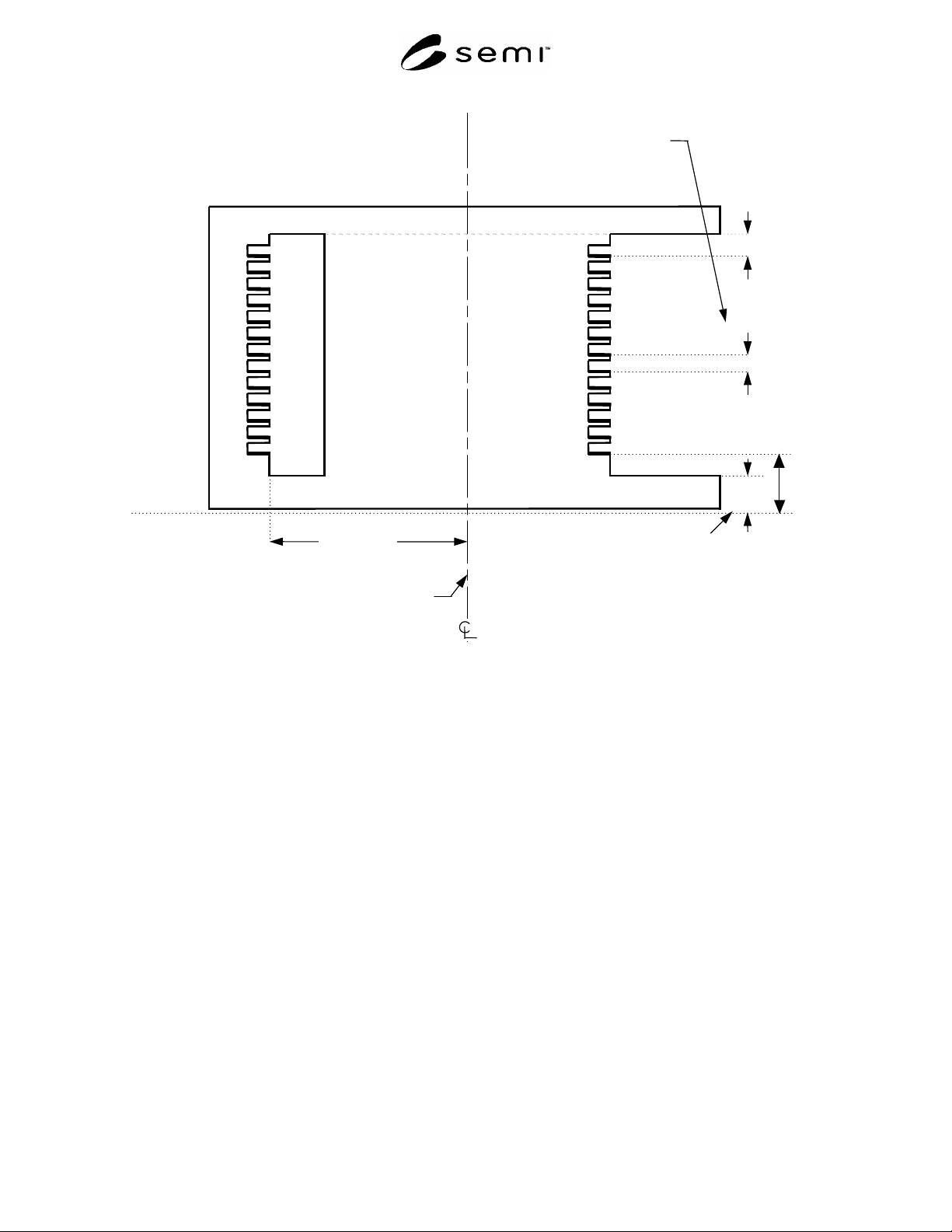
SEMI E119-1104 © SEMI 2002, 2004 5
horizontal datum plane
z8
=35
z6
28.5
z12
= 6.25
z15
4.6
facial datum plane
front side of the FOBIT where wafers
are accessed
y5 120
Figure 2
Side View of FOBIT Internal Dimensions
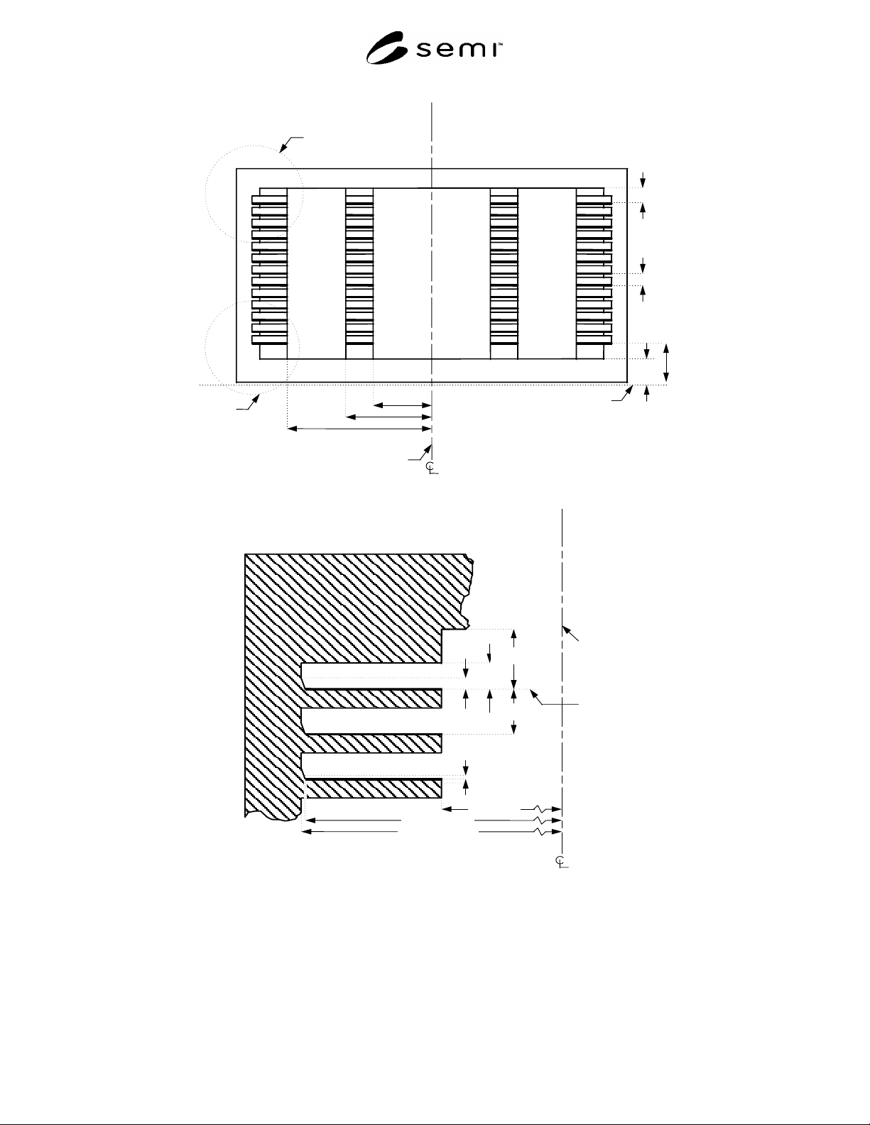
SEMI E119-1104 © SEMI 2002, 2004 6
z
4.6
x
1
50
x
2
75
x
3
125
Detail in
Figure 5
Detail in
Figure 4
horizontal datum plane
z 8
= 35
15
z 6
28.5
z
12
= 6.25
bilateral datum plane
Figure 3
Front View of FOBIT Internal Dimensions
z
23
1.5
z
11
2.9
z
12 = 6.25
x
3
125
bilateral
datum
plane
top
nominal
wafer
plane
z
z
10 = ± 0.5
(height of
wafer bottom)
r
2 = 152
r3
r2 + 1
+1
–0
z
15
4.6
Figure 4
Upper Cross-Section at Facial Datum Plane
5.7.1 Wafer Set-Down Volume — The open space for
the wafer set-down volume consists of a cylindrical
section with radius r2 and a main axis parallel to and y1
in front of the nominal wafer centerline. The top of this
cylindrical section is z11 above the nominal wafer-
seating plane and its bottom is z10 above the nominal
wafer-seating plane. The implications for wafer
positioning of the tolerance on r2 are as follows. The
wafers should be placed in the FOBIT within a circle of
radius corresponding to the smaller bound on r2 to
avoid touching the edge of the wafer to the side of the
FOBIT. Once the wafer has been placed, the FOBIT
SEMI E119-1104 © SEMI 2002, 2004 7
must not allow a wafer to move outside of a circle of
radius corresponding to the larger bound on r2. There
are two exceptions to this limit on wafer movement.
When the wafer is pushed toward the rear of the
FOBIT, the location of the wafer is defined by the
wafer pick-up volume (see Section 5.7.3). When the
FOBIT is gently tilted forward up to 45°, the wafers
may slide forward, but it is recommended that they not
extend further than y20 from the facial datum plane.
5.7.2 Wafer Extraction Volume — The open space for
the wafer extraction volume includes a cylindrical
section with radius r3 and a main axis parallel to and y1
in front of the nominal wafer centerline. The top of this
cylindrical section is z11 above the nominal wafer-
seating plane and its bottom is z23 above the nominal
wafer-seating plane. The wafer extraction volume also
includes the extrusion out the front of the FOBIT of this
cylindrical section. The implications for wafer
extraction of the definition of dimension r3 (r3 r2 +
1) are as follows; the FOBIT must give an extra 1mm
(0.04 in.) of horizontal clearance once the wafer is
picked up from wherever it ends up (within the bounds
of r2) after transport in the FOBIT.
5.7.3 Wafer Pick-Up Volume — If a wafer is placed in
the wafer set-down volume and is then pushed toward
the rear of the FOBIT, then the entire bottom of the
wafer must be contained in the wafer pick-up volume.
However, if the wafer is not pushed toward the rear of
the FOBIT, then the wafer may only be somewhere
within the wafer extraction volume. The wafer pick-up
volume is defined by a cylindrical section with radius
r1 and a main axis at the nominal wafer centerline. Its
top and bottom are the upper and lower tolerance of z10
around the nominal wafer-seating plane.
z
8 =35
x
3
125
z
12 =6.25
z
12 =6.25
bilateral
datum
plane
horizontal
datum plane
bottom
nom inal
wafer
plane
z
6
28.5
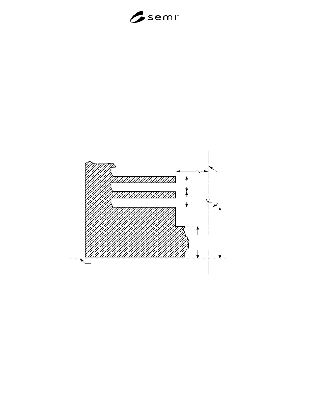
Figure 5
Lower Cross-Section at Facial Datum Plane