semi合集-English.pdf - 第6475页
SEMI G78-0699 © SE MI 1999 8 DIE Norm a lized Die Offset (No rmalized by Lo t) Averag e Die Of fset - Avera ge Lot Offs et [ACC URACY- TOTA L PROB E SYSTEM ERR OR] Thre e Sigm a Normalized Die Offset (No rmalized by Lo t…
SEMI G78-0699 © SEMI 19997
6.6.5 If the results of this method tu rn out to be
unfavorable, the user has the option of applying a more
detailed, enhanced data analysis application of this
method. That application is contained in Appendix 1.
The enhanced method uses the same data, but it
requires more manipulation of the data during data
analysis. The detail contained in the enhanced
algorithm will provide the user with greater insight as
to the cause of unfavorable results related to the probe
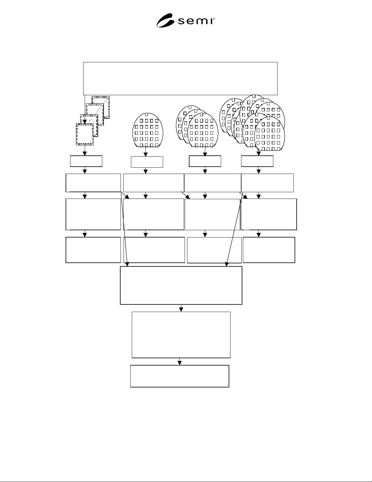
system under evaluation. A summary of the enhanced
method is shown in Figure 6.
6.7 Alternatives — What has been left undefined to
this point is availability of an automated approach to
data collection per the requirements of this method.
Regardless, data collection can be manually
accomplished. The manual process is laborious and
requires a video measuring system to make offset
measurements on the die pads, and a spreadsheet to
analyze the resulting data.
6.7.1 If manual operation is not desi rable or practical,
automated Probe Mark Analysis Systems do exist in the
market place as an item to be purchased. Providers are
also available to accept probed wafers and execute
probe mark analysis under contract as a service.
NOTE: A Final Note to the User of This Method — This
method provides sufficient data for sophisticated analysis of
probe system performance across die-to-die, wafer-to-wafer,
and setup-to-setup. It also provides a simple metric. It is easy
to make comparisons with simple "single number" metrics,
but that has the potential for oversight, distortion and
subsequent inappropriate comparisons. The test engineer,
working with the probe system supplier, must be the ultimate
judge of the applicability of this method and the correct
interpretation of the results.
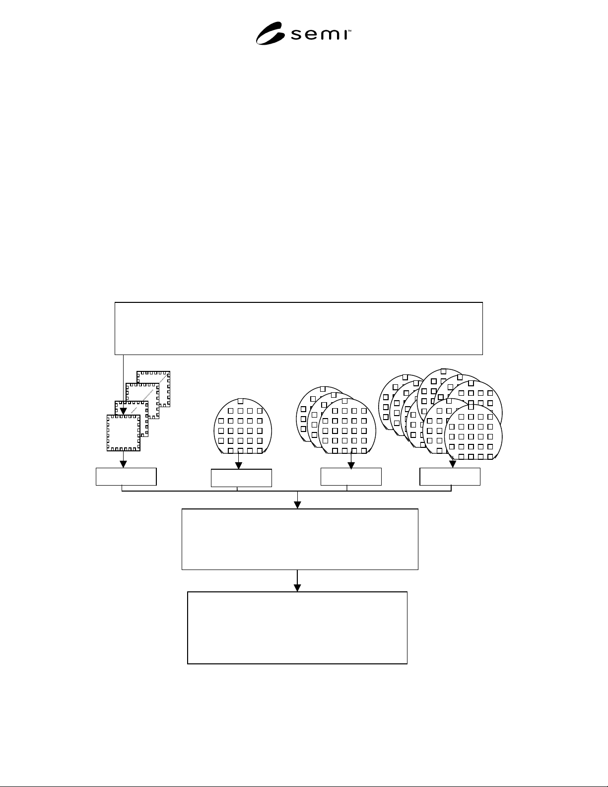
DIE
3
σ
σσ
σ
Average Die Offset
Three sigma calculation of Die Offset Values
Die to Die X and Die to Die Y variation
[REPEATABILITY]
VISION SYSTEM or PROBE MARK ANALYSIS SYSTEM
ESTABLISH
PAD OFFSETS
Offset from the center of the bond pad to the center of the scrub mark for Lot-X and Lot-Y
Average Die Offset
Average all Pad Offsets by die
(Avg. of 108 Lot-X and Avg. of 108
Lot-Y values)
SETUP LOT
1
2
WAFER
Figure 5
Pad Offset and Two-Step Analysis Algorithm for Determining Probe System Error
SEMI G78-0699 © SEMI 1999 8
DIE
Normalized Die Offset
(Normalized by Lot)
Average Die Offset - Average Lot Offset
[ACCURACY- TOTAL PROBE SYSTEM ERROR]
Three Sigma Normalized Die Offset
(Normalized by Lot)
Three sigma calculation of
Normalized Die Offset Value
[REPEATABILITY]
Three Sigma Total Probe System Error Range
Average Lot Offset +/- Total Probe System Error
VISION SYSTEM or PROBE MARK ANALYSIS SYSTEM
ESTABLISH
PAD OFFSETS
Offset from the center of the bond pad to the center of the scrub mark for all pads analyzed
Average Die Offset
Average all Pad Offsets by
die
Normalized Pad Offset
(Normalized by Die)
Pad Offset – Avg. Die
Offset
Three Sigma Normalized
Pad Offset
(Normalized by Die)
Average Wafer Offset
Avg. of Avg. Die Offset
Three Sigma Normalized
Die Offset
(Normalized by Wafer)
Normalized Die Offset
(Normalized by Wafer)
Avg. Die Offset – Avg. Wafer
Offset
Normalized Wafer Offset
(Normalized by Setup)
Avg. Wafer Offset – Avg.
Setup Offset
Three Sigma Normalized
Wafer Offset
(Normalized by Setup)
Normalized Setup Offset
(Normalized by Lot)
Avg. Setup Offset – Avg.
Lot Offset
Three Sigma Normalized
Setup Offset
(Normalized by Lot)
SETUP LOT
WAFER
1
2
Average Setup Offset
Avg. of Avg. Wafer Offset
7
3
8
4
5
6
9
Average Lot Offset
Avg. of Avg. Setup Offset
10
11
12
13
15
14
Figure 6
Pad Offsets and 15-Step Analysis Algorithm for Determining Probe System Error
SEMI G78-0699 © SEMI 19999
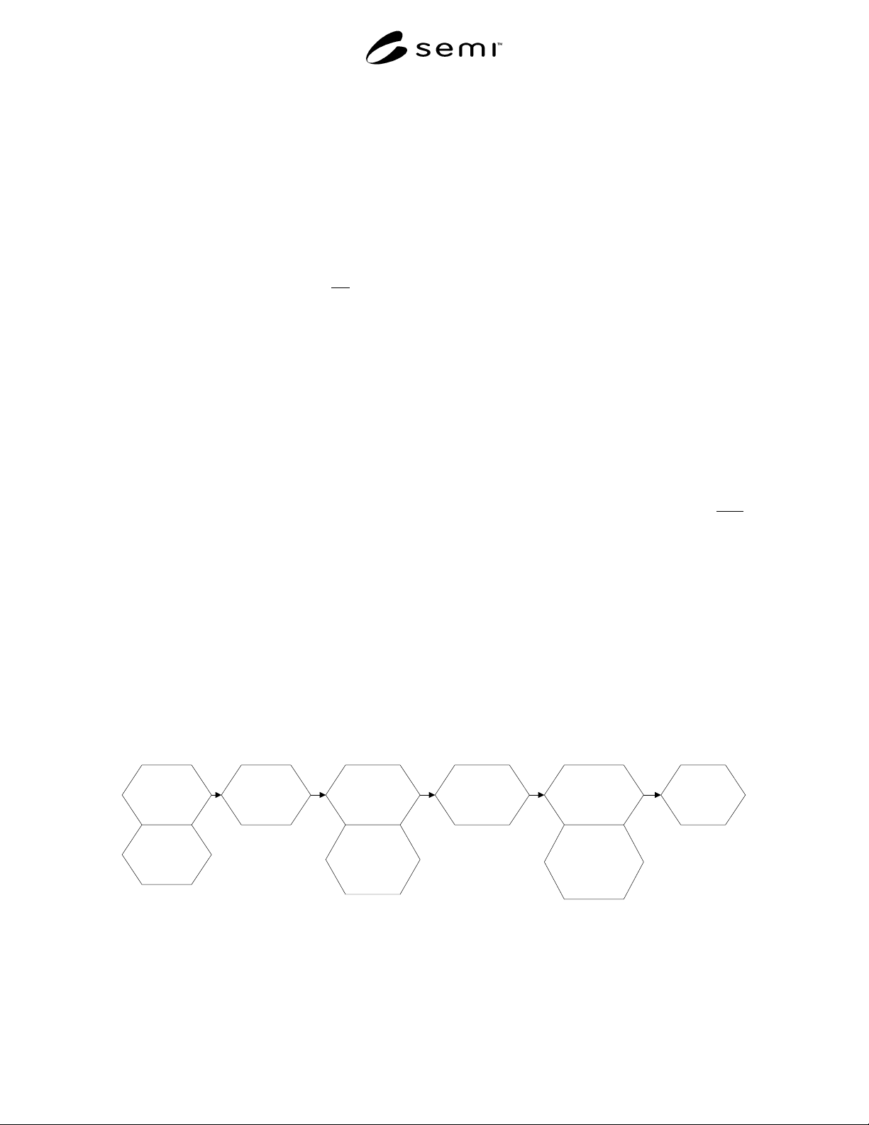
7 Required Hardware Check list (see Figure 7)
Wafer prober (if the test plan includes either hot or
cold chuck testing, the prober must be
appropriately equipped).
A planarized and aligned probe card which
matches the selected wafers, accompanied by a
metrology tool printout of the ‘x’, ‘y’ and ‘z’
positions of all of the probe tips to be used for
probe mark analysis. Note: The probe card should
be measured for alignment, but not ”tweaked”,
immediately prior to and after the conclusion of
each subsequent test.
Untested wafers
A special “test program” with a fixed “test” time.
Tester or PC that will run the “test program”. If a
PC is used to simulate the tester, it must be
equipped with the appropriate hardware for
communication with the wafer prober.
A stopwatch, with 0.1 second resolution. The
stopwatch is to have “split” capability.
Note that the user of this method may choose at
their discretion to utilize any other time stamp
logging technology at their disposal, so long as the
computational overhead of this logging has no
effect upon the throughput of the prober.
8 Requirements (see Figure 7)
8.1 Qualified Prober — Before initiating the test
process, the wafer prober is to be certified by a
representative of the prober manufacturer to be fully
operational.
8.2 Qualified Personnel — The individual running the
wafer prober for the test procedure must be certified or
otherwise qualified to operate the prober being tested.
9 Test conditions (see Figu re 7)
9.1 Test Time — a fixed “device te st time” will be
used during these tests. The recommended value for
this test time is 1.0 seconds.
9.2 Accuracy and Repeatability vs. Throughput — The
person or manufacturer running this test may make a
choice (or choices) as to how they elect to balance
accuracy and repeatability with throughput, but all three
tests must be run simultaneously. This will generate a
set of numbers defining a particular prober's accuracy
and repeatability at a given throughput (or a throughput
at a given accuracy and repeatability). All adjustments
to the prober are to be made using standard, end-user-
adjustable settings, and all prober settings associated
with a particular throughput / accuracy and repeatability
combination are to be included in the final report.
9.3 Temperature — This test can b e conducted at any
temperature, however, numerous variable can distort
the results if run at a temperature other than ambient,
i.e. probe tip drift due to an increase or decrease in
temperature.
• Cautionary Note: If the tests are performed at
temperatures other than ambient, the user must use
the same probe card and wafer type for all tests
across all test platforms to ensure uniformity of
results.
9.4 Probe Card Type — All types of probe cards
(blade, peripheral / cantilever or vertical) may be used,
so long as they leave a visible scrub mark.
• Cautionary note: Some vertical probe cards exhibit
an inherent amount of ‘x’ - ‘y’ needle drift. The
user should verify the intrinsic repeatability of the
probe card before using it to characterize the
prober.
Prober
available?
Probe card
available?
"Test
Program"
available?
Stop-
watch
available?
Is Prober
"Qualified"?
Condition of
probe card
known,
documented?
Personnel
"Qualified"?
Hardware to
run "Test
Program"
available and
tested?
Untested
wafers
available?
7.0 8.2 7.0
9.5
7.0 7.0
7.0
7.0
8.1
Figure 7
Preparation