semi合集-English.pdf - 第7457页
SEMI MF1535-1104 © SEMI 2004 15 RELATED INFORMATION 3 MINORITY-CARRIER RECOMBINATION LIFETIME NOTICE : This relat ed information is not an offici al part of SEMI MF1535. It was de rived from information developed during …
SEMI MF1535-1104 © SEMI 2004 14
comparable with p
0
(approaching the intrinsic
condition) and the carrier recombination lifetime
decreases; however, no single term dominates the
expression and so the slopes have no physical meaning.
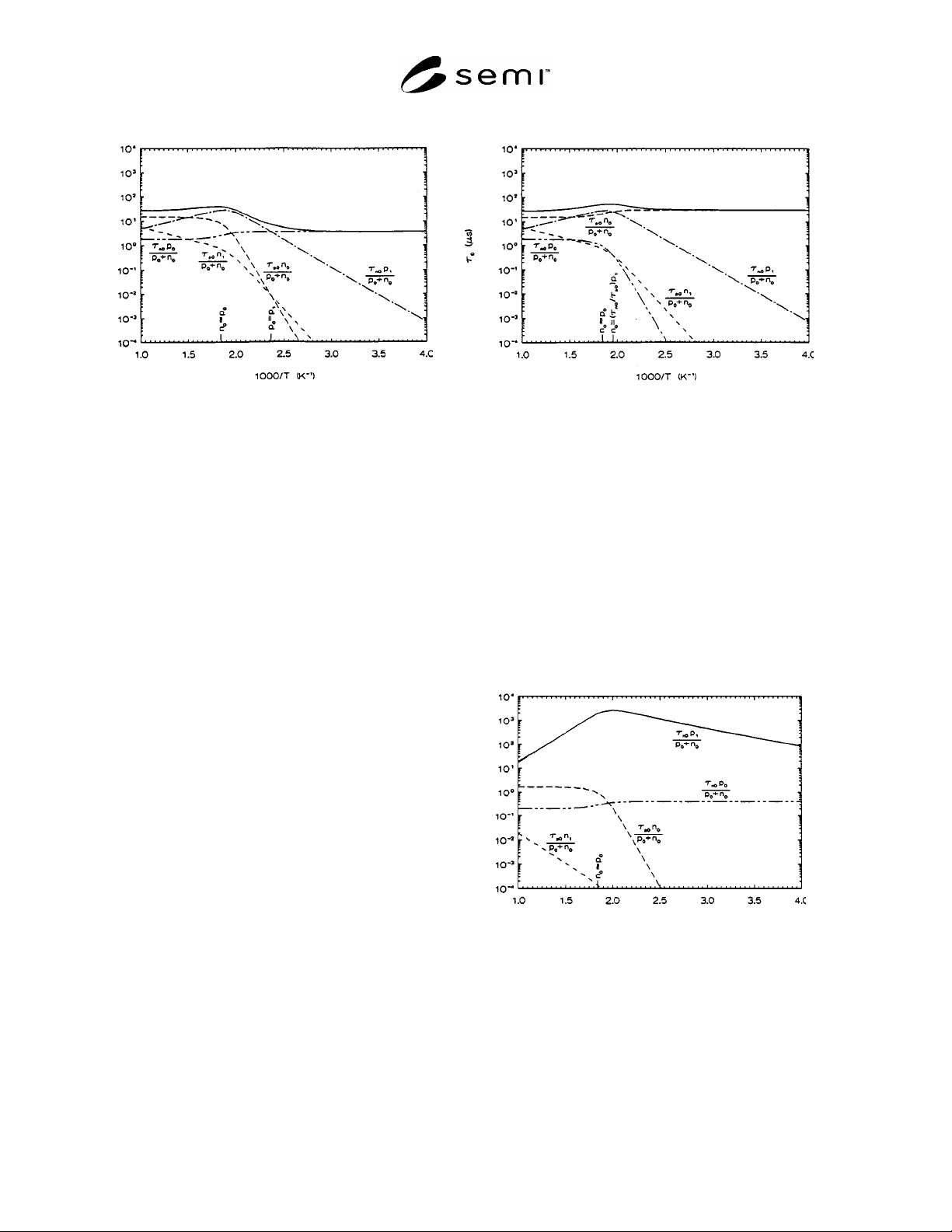
R2-4.2 Elemental Iron in n-Type Silicon (see Figure
R2-2) — Below about 100°C, n
0
>> p
1
>> n
1
>> p
0
, so
0
=
p0
. Between about 200°C and about 225°C, p
1
>
n
0
> p
0
and the term p
1
is again the largest single term.
In this case, there is even less difference between the
terms in
p
1
and p
0
, so the slope of the
0
curve is never
dominated by a single term, and thus the energy of the
elemental iron center cannot be determined from the
curve. At still higher temperatures, p
0
becomes
comparable with n
0
(approaching the intrinsic
condition) and the carrier recombination lifetime
decreases; however, as for near-intrinsic p-type
material, no single term dominates the expression and
so the slopes have no physical meaning.
R2-4.3 Iron-Boron Pairs in p-Type (Boron-Doped)
Silicon (see Figure R2-3) — In this case, p
1
>> p
0
>>
n
0
>> n
1
, so that the term in p
1
dominates the low-
injection recombination lifetime at all temperatures
from well below room temperature to about 225°C.
Since
p
0
= N
boron
,
0
n0
(p
1
/N
boron
), so that the negative
slope of a plot of ln
0
against 1/T yields
=
FeB
v
,
the activation energy of the iron-boron pair. At higher
temperatures, the material becomes near-intrinsic and
the denominator increases, resulting in a decrease in
0
.
R2-5 These examples illustrate the limited range of
conditions over which the activation energy obtained
from measurements of carrier recombination lifetime as
a function of temperature slightly above room
temperature can be associated with the energy level of a
defect center located near the middle of the forbidden
energy gap, as are most of the elemental metallic
impurities.
Figure R2-3
Low-Injection Recombination Lifetime (solid curve)
as a Function of Reciprocal Temperature for Iron-
Boron in p-Type Silicon
Figure R2-1
Low-Injection Recombination Lifetime
(solid curve) as a Function of Reciprocal
Temperature for Elemental Iron in
p-Type Silicon
Figure R2-2
Low-Injection Recombination Lifetime
(solid curve) as a Function of Reciprocal
Temperature for Elemental Iron in
n-Type Silicon

SEMI MF1535-1104 © SEMI 2004 15
RELATED INFORMATION 3
MINORITY-CARRIER RECOMBINATION LIFETIME
NOTICE: This related information is not an official part of SEMI MF1535. It was derived from
information developed during the original preparation of the standard in ASTM Committee F-1 in 1994.
This related information was approved for publication by full letter ballot procedures.
R3-1 The recombination of an excess electron-hole
pair at a defect center is a two-step process. It involves
either (a) the capture of an electron in an empty defect
center followed by the capture of a hole or (b) the
capture of a hole on a filled defect center followed by
the capture of an electron. Thus, the recombination
time depends on the number of filled or empty defect
centers as well as the capture time constants.
R3-2 The occupancy of the defect centres is controlled
by the position of the Fermi energy as discussed by
Blakemore.
16
If all of the defect centers are empty, the
electron recombination time is governed by the electron
capture time constant,
n0
; this occurs when the Fermi
energy is well below the defect center energy. If all of
the defect centers are filled, the hole recombination
time is governed by the hole capture time constant,
p0
;
this occurs when the Fermi energy is well above the
defect energy. Since the position of the Fermi energy is
governed primarily by the dopant density, the
occupancy of the defect centers may be different for
different resistivity wafers.
R3-3 There are two sets of equivalent cases. The
defect center may be in the same half of the forbidden
gap as the Fermi energy or it may be in the other half.
Thus, the case for the defect center in the lower half of
the gap of a
p-type semiconductor is the same as for the
defect center in the upper half of the gap in an n-type
semiconductor with the roles of electrons and holes
interchanged. Similarly, the case for the defect center
in the upper half of the gap in a p-type semiconductor is
the same as for the defect center in the lower half of the
gap in an n-type semiconductor.
R3-4 As examples, consider the three cases of
elemental iron in both n- and p-type silicon and iron-
boron pairs in p-type silicon at room temperature (300
K). In each case the iron density is assumed to be
5 × 10
11
atoms/cm
3
. Note that at for very low resistivity
wafers, the nondegeneracy requirement of the S-R-H
model may be violated.
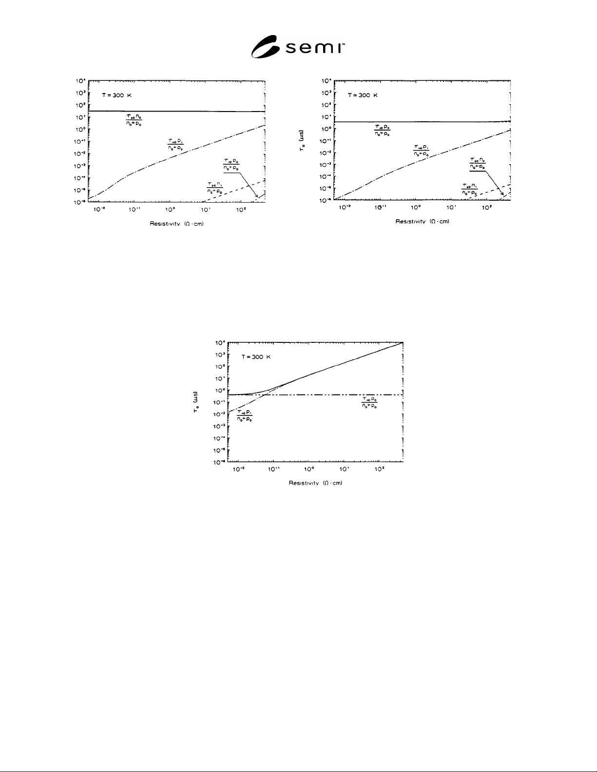
R3-4.1 Elemental Iron in p-Type Silicon (see Figure
R3-1) — For all practical values of resistivity, the
Fermi energy lies many kT below the near mid-gap
energy of the elemental iron center. Consequently, the
defect centers are empty and the limiting process is
capture of excess minority electrons, there being ample
numbers of holes present to recombine with the electron
immediately upon its capture by the defect center.
Therefore, the small-signal carrier recombination
lifetime is equal to the electron (minority-carrier)
capture time constant:
0
=
n0
.
R3-4.2 Elemental Iron in n-type Silicon (see Figure
R3-2) — In this case, for all values of resistivity, the
Fermi energy is very far above the defect center energy
and all the defect centers are filled, and hole capture is
governed by the hole capture time constant,
p0
.
Because the Fermi energy is close to the conduction
band edge, there are large numbers of electrons present
so that as soon as a hole is captured, the defect center is
filled again. Therefore, hole capture is the limiting
process, and the small-signal carrier recombination
lifetime is equal to the hole (minority-carrier) capture
time constant:
0
=
p0
.
R3-4.3 Iron-Boron Pairs in p-Type (Boron-Doped)
Silicon (see Figure R3-3) — This defect center is
located quite close to the valence band edge. For all but
very low resistivity wafers, the Fermi energy lies above
the defect center energy so that some of the defect
centers are filled. In this case, the capture of minority
electrons is still the limiting process, but since only a
fraction of the sites can capture an electron, the small-
signal recombination lifetime is larger than the electron
capture time constant. Quantitatively, because
n
0
<< p
0
,
the small-signal carrier recombination lifetime is given
by
0
=
n0
(p
1
/p
0
).
R3-4.4 The fourth possible case is one in which the
defect center is located near valence band edge in n-
type material. The iron-boron pair, of course, cannot
exist in n-type material; however, for the case of a
hypothetical defect center with energy near the valence
band in n-type material,
n0
p
1
>>
p0
n
0
for all but the
most heavily doped material so this term dominates the
small-signal lifetime and the minority-carrier properties
do not influence the recombination process.
R3-5 Thus, for deep lying defect centers, the low-
injection (small-signal) carrier recombination lifetime is
equal to the minority-carrier capture time constant (or
minority-carrier lifetime), while for centers close to the
band edge, the small-signal carrier recombination
lifetime can be much larger than the minority-carrier
capture time constant.
SEMI MF1535-1104 © SEMI 2004 16
Figure R3-3
Low-Injection Recombination Lifetime (solid curve)
as a Function of Resistivity for Iron-Boron Pairs in
p-Type Silicon at Room Temperature
Figure R3-2
Low-In
j
ection Recombination Lifetime (solid
curve) as a Function of Resistivity for
Elemental Iron in n-Type Silicon at Room
Temperature
Figure R3-1
Low-In
j
ection Recombination Lifetime (solid
curve) as a Function of Resistivity for
Elemental Iron in p-Type Silicon at Room
Temperature
NOTICE: SEMI makes no warranties or representations as to the suitability of the standards set forth herein for any
particular application. The determination of the suitability of the standard is solely the responsibility of the user.
Users are cautioned to refer to manufacturer's instructions, product labels, product data sheets, and other relevant
literature, respecting any materials or equipment mentioned herein. These standards are subject to change without
notice.
By publication of this standard, Semiconductor Equipment and Materials International (SEMI) takes no position
respecting the validity of any patent rights or copyrights asserted in connection with any items mentioned in this
standard. Users of this standard are expressly advised that determination of any such patent rights or copyrights, and
the risk of infringement of such rights are entirely their own responsibility.
Copyright by SEMI® (Semiconductor Equipment and Materials
International), 3081 Zanker Road, San Jose, CA 95134. Reproduction of
the contents in whole or in part is forbidden without express written
consent of SEMI.